Ray Wilson authored this content while he was actively running MFOS as the founder and resident genius.
We retain the content because it reflects a valuable point of view representing that time and place.
Article by Ray Wilson
Introduction
Often in synth-DIY trouble-shooting and/or circuit experimentation, a signal source with variable frequency and amplitude is just what you need to test a circuit’s behavior. If the signal source has a variety of wave-shapes, it will serve in more scenarios. This article will present a 9V battery-powered function generator that outputs sine, square, and triangle waveforms. The frequency is adjustable from about 20 Hertz to about 11KHz and the output level can be varied from 0 to about 3V, peak to peak. I kept the output level within this range as the circuit is essentially powered by a virtual +/-4.5V power supply and I wanted the unit to continue to function as long into the 9V battery’s depletion as possible. The circuit drains about 11mA when used with the LED shown in the schematic. However, if you buy a power switch with an obvious passive indication of state, you can leave the LED off and the circuit will draw about 9mA. In either case, you can count on a good long life on a 9V alkaline battery. The signal can be injected into the input of a VCF or VCA circuit under development or a mixer or an amplifier input you want to test. Since it’s battery powered you can leave one in your toolbox.
Capacitor C2 may have the value .002uF or .0022uF.
9V Battery Powered Function Generator Schematic
View as PDF
9V Battery Powered Function Generator Circuit Description
A little housekeeping info first: In my schematics, a circle with letters in it is used to indicate both intra-page and extra-page connections. Consider all circles with the same letters connected together (even across pages in a multi-page schematic). If I showed all those points running back to the power supply, the schematic would be really hard to read. The circuit points labeled with Xn or other tokens (e.g. TRI, OUT, X1) connect from the circuit board to the panel components. You will see these names again when you look at the panel wiring diagram. I use the straight and curved line capacitor symbol for all capacitors. If a capacitor is polarized, I add a + (plus) symbol next to the straight line in the capacitor symbol (e.g. C1, C3).
Let’s look at how this circuit works. We’ll start with the simple battery power supply. We split the battery’s voltage in half with two 4.7K resistors: R1 and R3. The unit’s virtual ground will come from the junction of the two resistors. The best way to understand this is to see the supply as delivering plus 4.5V from the battery’s positive terminal, minus 4.5V from the battery’s negative terminal, and a virtual ground from the junction of resistors R1 and R3. The 220uF aluminum electrolytic capacitors C1 and C3 are used as charge reservoirs for the two halves of the supply. The points BP (battery positive) and BN (battery negative) indicate the power supply connections throughout the schematic. The two points also labeled BP and BN are PC board donut labels to which the battery’s power, after being switched via S1, is applied.
To LED or not to LED, that is the question. While LEDs suck power, so does forgetting to turn the unit off. The choice is yours. Use a switch that has a nice “on” state indication and remember to turn the power off—or use a LED’s cheerful glow to remind you that the unit is on and use a bit more current—but remember to turn it off.
So, if you use LED1, it simply illuminates due to being forward-biased when the unit’s power is turned on. Use a high efficiency LED because it’s not getting a lot of current, but you’ll see it for sure. If you want LED1 to be brighter (and the battery to die sooner) reduce the value of R2 to, say, 2K or maybe 1.5K.
We are using U1-A (1/4 TL074 Quad Op Amp) as an integrator and U1-B (1/4 TL074 Quad Op Amp) as a comparator. Together they make up the heart of the function generator’s oscillator. On power-up, the output of U1-B (our comparator) will always be either saturated high or saturated low. We’ll consider that it powered-up saturated low as we discuss its operation. On power-up, the output of the op amp used as our integrator (U1-A) will be at ground level, but will immediately start to ramp high under the influence of U1-B’s output. U1-B’s low output is fed back to its non-inverting input through series connected 62K resistors R5 and R6. Two 1N914 diodes are connected between the R5/R6 junction and ground. D1's cathode is connected to the R5/R6 junction and D2's anode is connected to the R5/R6 junction. The other ends of the diodes are connected to the circuit’s virtual ground (we’ll just say ground from now on).
What are diodes D1 and D2 doing? They are controlling the voltage at the R5/R6 junction so that as U1-B’s output changes from positive saturation to negative saturation, the voltage at the R5/R6 junction changes from a forward diode drop above ground (about +600mV) to a forward diode drop below ground (about -600mV).
We do this so that the voltage fed back to the integrator is the same magnitude in both directions. The reason we don’t just use the output of U1-B is because its positive and negative saturation voltages are not quite the same. Since the current fed to the integrator via the Fine and Coarse Frequency controls and R10 depends on the magnitude of the voltage coming from the comparator section, it is important that the voltage be the same in the positive and negative directions or else the integrator’s triangle wave-shape will suffer from poor side-to-side symmetry. Instead of looking triangular, the wave would appear skewed (more sawtooth or ramp wave looking).
The low initial level on the output of U1-B results in current flowing from the inverting input of the integrator U1-A pin 2 (via 62K resistor R10, 100K coarse frequency pot R9 and 100K fine frequency pot R4) toward the -600mV voltage level at the R5/R6/D1-k/D2-a junction.
In response, the output of the integrator (U1-A pin 1) ramps up until the current flowing into comparator U1-B’s non-inverting input via 180K resistor R7 overcomes the current flowing towards the -600mV level on the R5/R6/D1-k/D2-a junction via 62K resistor R5.
When the output of U1-A ramps high enough (about +1.7V), the output of comparator U1-B switches to positive saturation. Now the R5/R6/D1-k/D2-a junction level is at +600mV and current flows toward U1-A’s inverting input via R4, R9, and R10. The output of the integrator ramps low until its voltage is low enough (about -1.7V) to pull enough current through R7 to overcome the current flowing through R5 from the +600mV level at the R5/R6/D1-k/D2-a junction. At that time, the output of the comparator shoots rapidly to negative saturation and the process continues resulting in triangle-wave oscillation at the output of integrator U1-A and square wave oscillation at the output of comparator U1-B.
The 100K Coarse Frequency potentiometer R9 is used as an adjustable voltage divider to control the level of the voltage, which causes current to flow into or out of R10 and subsequently into or out of the inverting input of the integrator. When R9's wiper is adjusted in the direction of R4, the input of the integrator sees more voltage (thus current) and the frequency goes higher. When R9's wiper is adjusted toward R13, the input of the integrator sees less voltage (thus current) and the frequency is lower. Resistor R13 (3K) sets the limit for how low the voltage can be adjusted and still cause the integrator to ramp properly when potentiometer R9 is adjusted all the way down.
The 100K Fine Frequency control (R4) simply allows more or less current to flow between the output of the integrator section and the inverting input of the comparator as it is adjusted. It is optional and can be eliminated if you don’t need fine frequency control. If R4 is not used, simply connect point X1 to the top of potentiometer R9's resistive element.
Switch S2 is used to connect a larger capacitor (C2 .0022uF) in parallel with C4 (100pF) in order to change the range of the oscillator from high (S2 open) to low (S2 closed). When a larger capacitor is used in an integrator, the ramp rate becomes lower. When S2 is open, the function generator’s frequency range is about 400 Hz to 10KHz. When S2 is closed and C2 is in parallel with C4, the frequency range is lowered to about 16Hz to 590Hz Thus the function generator has a nice wide range of frequency adjustment.
We see a nice triangular wave-shape at the output of U1-A (circuit point TRI) that oscillates about the unit’s virtual ground with an amplitude of about 3V, peak to peak. We take the square wave appearing on the output of U1-B and reduce its amplitude to about 4V peak to peak while maintaining a low impedance source by using U1-C to apply fractional inverting gain (circuit point SQR). The 22pF ceramic capacitor across resistor R15 is there to reduce a slight rising edge ringing that appears on the output of U1-C without it.
To simplify the circuit and lower current consumption a bit, you can eliminate the sine wave functionality if desired. Simply eliminate the LM13700 and associated components and change the output wave selection switching to only select between square or triangle waves. You’ll use one less SPDT switch as well.
However, I find the sine wave useful for trouble-shooting, which is why I included it. To change the triangle wave into a sine approximation, we overdrive the non-inverting input of U2-A LM13700 Dual Transconductance Op Amp to take advantage of the non-linear distortion it provides. This distortion tends to curve the top and bottom of the triangle waveform inward, giving it a sinusoidal appearance. The triangle waveform is fed from the output of U1-A to the non-inverting input of U2-A (pin 3) via 100K trim pot R16. Trim pot R16 is used to adjust the amplitude of the signal appearing at U2-A’s non-inverting input.
We are purposely over-driving the input so R16 adjusts the amount of distortion the signal undergoes. Too little and the signal looks triangular; too much, and the signal looks too flat on the top and bottom.
You’ll be able to see (and hear) when it’s just right. The 100K trim pot R24 is used to apply an adjustable bias current to the non-inverting input via 200K resistor R19. Thus trimmer R24 is used to adjust the top to bottom symmetry of the sine wave-shape. The 100K trim pot R17 is used to apply the bias signal to the transconductance op amp U2-A and thus controls the amplitude of the sine wave-shape. We use the darlington buffer amp provided on the LM13700 chip to buffer the output.
Resistors R22 (220K) and R23 (680K) bias the output of U2-A so that the sine wave oscillates about the unit’s virtual ground. Resistor R18 (10K) converts the current from U2-A pin 8 to voltage. The SIN circuit point comes from U2-A pin 8. The other half of U2 (U2-B) is not used in this circuit.
The SQR, TRI, and SIN circuit points are switched via S3 (SPDT switch) and S2 (SPDT switch) and dropped across R11 (100K potentiometer) that is used as an adjustable voltage divider. The portion of the selected waveform picked off of R11's wiper is applied to the inverting input of U1-D via 10K resistor R12. U1-D’s 12K feedback resistor gives it a gain of 1.2, which gives each waveform a bit of amplification. This scheme delivers the level adjusted selected waveform from the low impedance output of U1-D.
Capacitors C6 through C9 are .1uF ceramic caps that should be placed close to the power pins of both ICs (U1 and U2) during circuit construction.
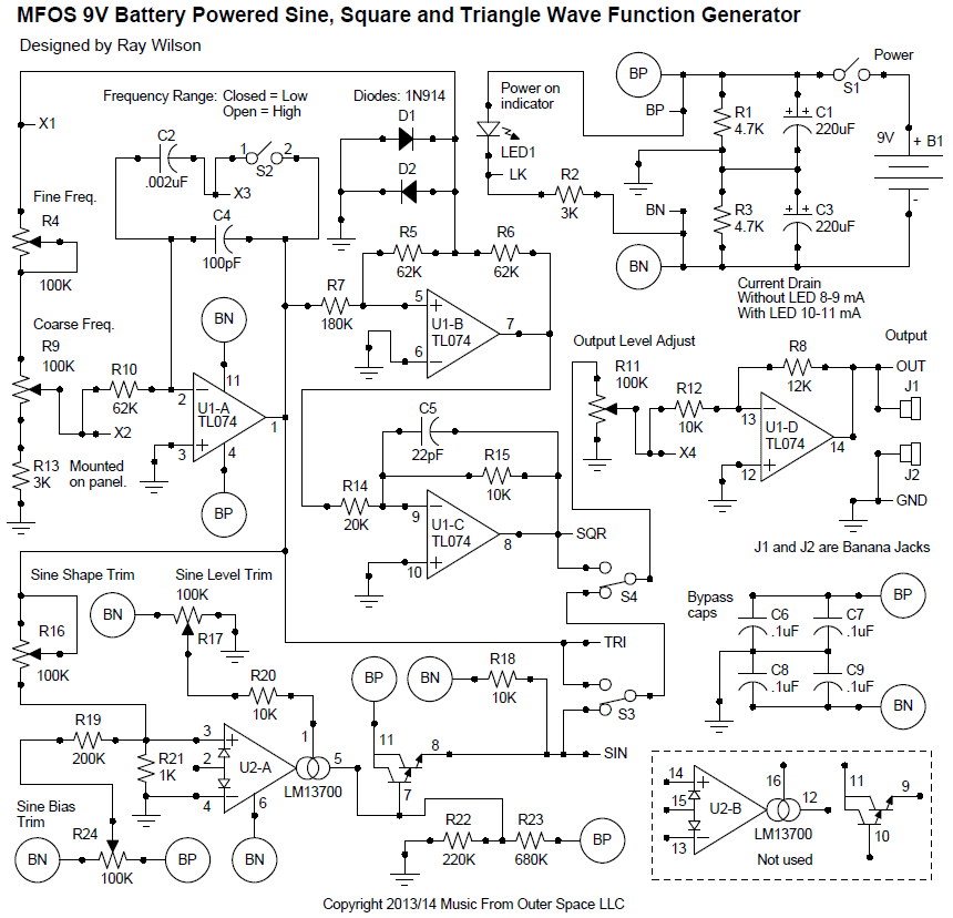
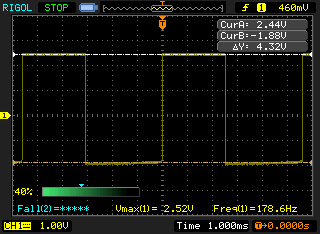
Scope Photos
Your waveforms should look like this.
| Square wave at max output. | Triangular wave at max output. | Sine wave at max output. |
 |
 |
 |
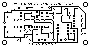
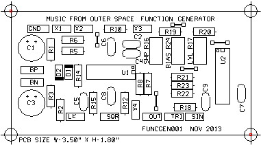
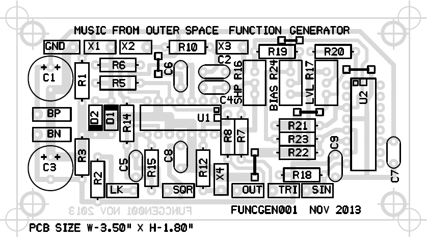
Double Sided PC Board Info (MFOS sells this version of the PC board.)
Bottom copper is as viewed from the top of the PC board.
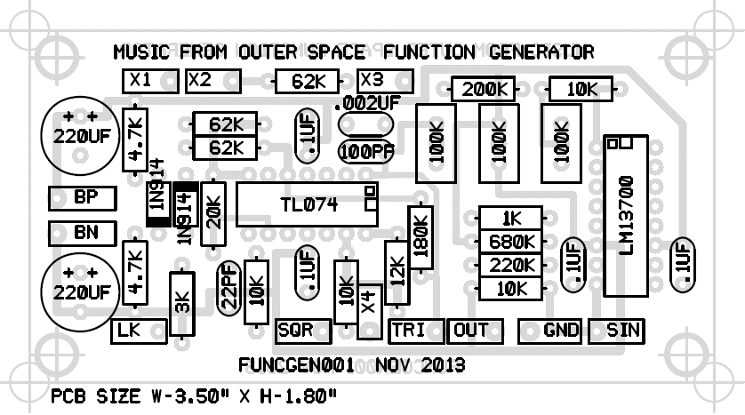
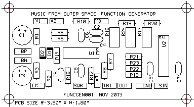
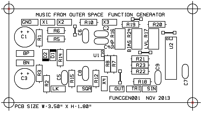
PCB Showing Component Values
This view is handy for the board population stage. You won't need to refer back and forth to the schematic while inserting components - just use this chart.
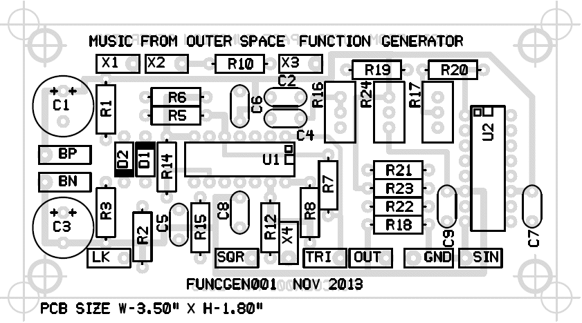
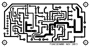
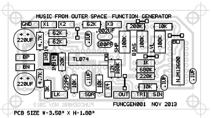
PCB Showing Component Designators
This view is handy for the project trouble shooting stage. You can refer to the schematic and then easily find any component by its designator.
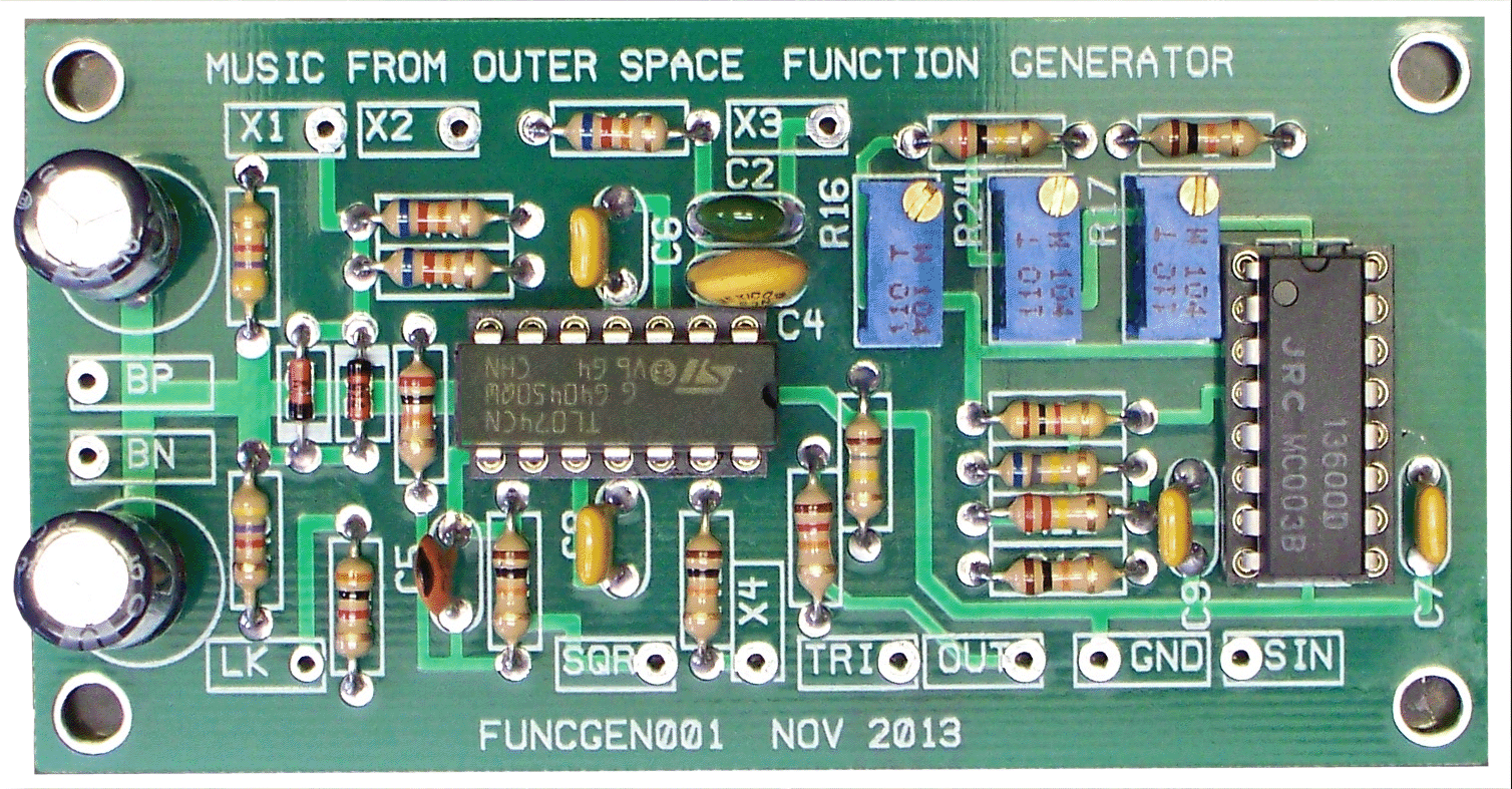
Populated PCB
After component population your board should look similar to this.
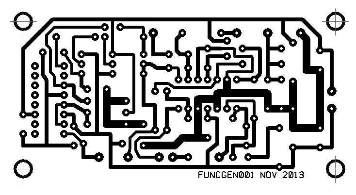
PCB Top Copper
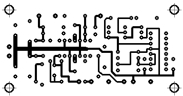
PCB Bottom Copper (as viewed from the top of the PC board)
PCB Legend Silk Screen
Constructing the Battery Signal Generator
This is the conclusion to my last article "Make a 9V Battery Powered Function Generator". The schematic and the circuit description were presented in that article. In this article I present some construction tips and drawings to help you actually build and use the circuit. Sorry for the delay between articles but I was working on designing two new products involving delay chips.
As mentioned in the last article, you'll need a case to put the battery signal generator in and a faceplate to hold the front panel controls. I'm no case guru so I'm leaving the case construction to you. Buy a Radio Shack case, or maybe a Hammond case, a BUD box, a cardboard box, or a nice wooden box you make in your shop. As long as the front plate can hold the controls you should be fine. I prefer conductive material for faceplates because it grounds all of the pot bodies and reduces noise in the system. Run a ground wire from the faceplate to the circuit's ground for best results. I'll show you where in the following information.
Although I sell double sided PC boards for my projects (including this one at MFOS) I know it is easier for hobbyists at home to make single sided PC boards. The following board layout is sized for 1 to 1 contact artwork. If the art does not print so that you have 1/10" between adjacent IC pads and 3/10" between IC pads across from one another try adjusting the pixels/inch of your art program until it does. I'm not an art program expert and the patterns print correctly for me on my laser printer so I wish I could give more help there but... I can't. I've included a 2X pattern as well in case it comes in handy. The component legend silk screen pattern is there for the die-hard home screen printers. I know how it is. I used to do it. A word to the wise - be careful with the chemicals involved in board making and screening processes. Wear gloves, goggles, have good ventilation and dispose of things properly. You'll be glad you did.
Single Sided PC Board Info (For home hobbyists who make PC boards.)
Single Sided PCB Bottom Copper (as viewed from the bottom of the PC board)
X2 Artwork (as viewed from the bottom of the PC board)
Single Sided PCB Legend Silk Screen (as viewed from the top of the PC board)
Here is a view of the values that go at each of the legend locations on the PC board. This view is handy for the board population stage. You won't need to refer back and forth to the schematic while inserting components - just use this chart. Double check that you've put a resistor or capacitor in every location or you'll be trouble-shooting later. Make sure you solder every solder joint as well or... you guessed it trouble-shooting again. I've highlighted the fact that you must install a wire jumper in the four locations inidacted on the PC board. This is normally a piece of 22 to 24 gauge solid copper wire bent to fit the holes. Trimmed off resistor leads often work well.
Single Sided PCB Showing Component Values
This view is handy for the project trouble shooting stage. You can refer to the schematic and then easily find any component by its designator. Working your way through the circuit requires that you be able to locate all of the electronic components shown in the schematic and this is your map to know which is which.
Single Sided PCB Showing Component Designators
Front Panel Layout And Wiring
View as PDFI show three views of the front panel below. The conceptual view shows the panel with it's controls. The mechanical view is used as a hole pattern. You lay it over the material you plan to use for your front panel and then use a center punch to make drill guide divots. The wiring view shows both the interconnections for the panel controls and the points on the front panel that connect to the PC board. The "Xn" designators on the PC board are external connection points.
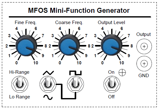
Conceptual View
Its always a good idea to think about your front panel and to make a mock up drawing so that you don't forget a control you may want and so you can arrange the panel logically. You can cut and paste using any art program to come up with a conceptual drawing for your control panels.
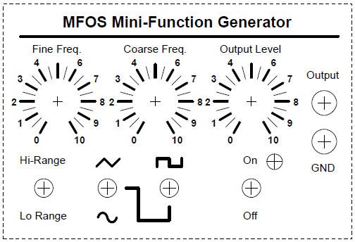
Mechanical View For Fabrication
Print a copy of this for use as a drill hole guide. I like to tape mine squarely to the material I'm using for the front plate and then use a sharp center punch to make drill guides at every place I plan to drill a hole. Be sure to use the correct drill size for the components you mount. The potentiometers and banana jacks usually fit in 5/16" holes, the mini-toggle switches normally fit in 1/4" holes. Size the LED's mounting hole for the type you buy. The regular sized ones (good old fashioned LEDs) are typically 0.2" (5mm) in diameter.
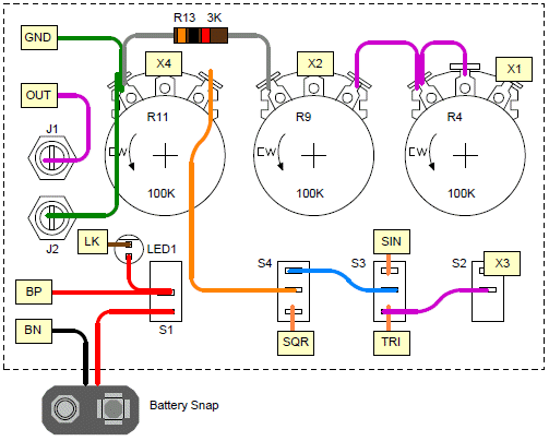
Wiring View
I find that 22 to 24 AWG size stranded wire works well for panel wiring. First solder the wires (or flying components) that run between panel components. Next wire each labeled PC board port (donut pad with an Xn label near it) to the corresponding Xn point on the front panel diagram as indicated. This is where 90% of the trouble shooting issues are born so check your wiring carefully - then check it again.
Component List (BOM)
Component Notes
All cap voltages should be 25V or more. Film or ceramic caps will work fine for the non-electrolytic caps. All resistors are 1/4W 5% (1% will work fine). MFOS PC boards use dual inline IC packages. MFOS PC boards usually use 5mm (0.2") cap lead spacing unless it is obvious from the board's legend that it should be larger or smaller.
| Qty. | Description | Value | Designators |
|---|---|---|---|
| 1 | LM13700N Dual Transconductance Op Amp | LM13700N | U2 |
| 1 | TL074CN Quad Op Amp | TL074CN | U1 |
| 2 | 1N914 Sw. Diode | 1N914 | D1, D2 |
| 1 | General Purpose LED | LED | LED1 |
| 3 | Linear Taper Potentiometer | 100K | R4, R9, R11 |
| 4 | Resistor 1/4 Watt 5% | 10K | R12, R15, R18, R20 |
| 1 | Resistor 1/4 Watt 5% | 12K | R8 |
| 1 | Resistor 1/4 Watt 5% | 180K | R7 |
| 1 | Resistor 1/4 Watt 5% | 1K | R21 |
| 1 | Resistor 1/4 Watt 5% | 200K | R19 |
| 1 | Resistor 1/4 Watt 5% | 20K | R14 |
| 1 | Resistor 1/4 Watt 5% | 220K | R22 |
| 2 | Resistor 1/4 Watt 5% | 3K | R2, R13 |
| 2 | Resistor 1/4 Watt 5% | 4.7K | R1, R3 |
| 3 | Resistor 1/4 Watt 5% | 62K | R5, R6, R10 |
| 1 | Resistor 1/4 Watt 5% | 680K | R23 |
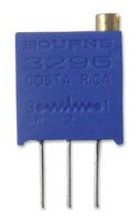
| 3 | Trim Pot (Bourns 3296W or equivalent) | 100K | R16, R17, R24 |
| 1 | Capacitor Ceramic | .0022uF | C2 |
| 4 | Capacitor Ceramic | .1uF | C6, C7, C8, C9 |
| 1 | Capacitor Ceramic | 100pF | C4 |
| 1 | Capacitor Ceramic | 22pF | C5 |
| 2 | Capacitor Electrolytic | 220uF | C1, C3 |
| 2 | SPDT Switch | SPDT | S3, S4 |
| 2 | Switch SPST | SPST | S1, S2 |
| 2 | Banana Jack | Banana Jack | J1, J2 |
| 1 | Battery | 9V Battery | B1 |
| 1 | Radio Shack Project Enclosure (6x4x2") | Cat#: 270-1806 | |
| 1 | Radio Shack 9V Snap Connectors | Cat#: 270-324 | |
| 1 | 25' Roll of 22 AWG Stranded Wire | 25 Feet | |
| 3 | Potentiometer Knobs | Knobs for Potentiometers |
Putting it All Together
Gather all required components for the project.
I suggest you shop online unless you have a local component store with good selection and pricing. Just search for electronic components and you'll find hundreds of online retailers. Shop around as prices can vary widely. Use 1/4 watt resistors and capacitors with at least 25V ratings and 5mm (0.2") lead spacing. Use trimmers that are physically similar to BOURNS 3296W style. They look like this and are sold at Tayda.
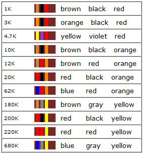
Resistor Color Chart For Resistors Used In This Project
Possible Capacitor Markings
Capacitors come marked in several ways. The capacitors that are used in this project may be marked as follows:| Value | Possible Marking 1 | Possible Marking 2 |
| .0022uF | 222 | 2.2nF |
| .1uF | 104 | 100nF |
| 100pF | 101 | |
| 22pF | 220 | |
| 220uF |
Populate the PC Board
Populate the PC board inserting and soldering lower profile components before higher profile components. For example begin with wire jumpers, next resistors, then IC sockets, finally any remaining components.Print Faceplate Template
Print the faceplate template and use it as a model to fabricate a faceplate. Fabricating the faceplate can be done using 1/16" sheet aluminum or other material but I recommend that it is conductive material. Using one of those project boxes that come with an aluminum faceplate should work perfectly.Populate Panel
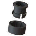
Insert the panel components onto the faceplate (pots, switches, LED, banana jacks). Align them the way the wiring diagram shows and make sure to tighten the mounting nuts. Some crazy glue can be used to mount the LED in it's hole or you can purchase a plastic LED clip-n-ring set with which to mount the LED. The LED clip-n-ring style holder looks like this.
The clip inserts into the LED's hole from the front of the panel, the LED is inserted into the clip from behind the panel. Finally the ring is snapped over the part of the ring sticking through the back of the panel which locks the LED in place. Drill the LED's mounting hole keeping the size of the particular LED and clip-n-ring set you buy in mind.
Test Leads
I recommend that your test leads be as simple as two wires with a banana jacks on one end and an alligator clip on the other. Kits come with two sets of banana jacks, banana plugs and insulated alligator clips in red and black. Red is usually used as the "hot" lead of the output and black as the neutral.
| Attaching the banana jack to stranded 22 gauge wire is simple. Strip the wire about 1.25" so you have enough to wrap around the banana jack. | 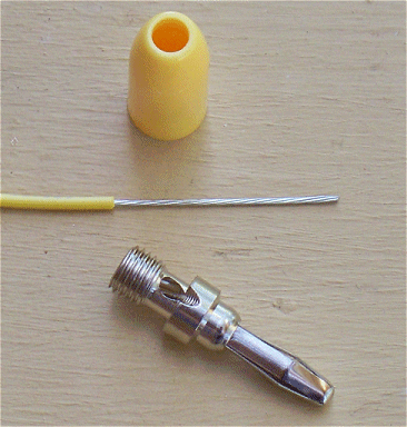 |
| Insert the wire into the hole in the banana jack as shown. If you have something on the other end of the wire already don't forget to put the insulator on the wire before threading the wire through the jack. I've pulled that one a time or two. | 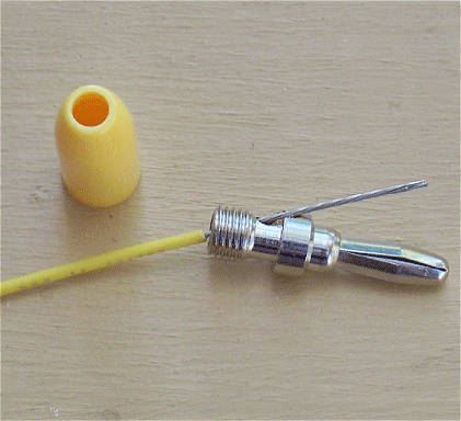 |
| Some folks solder them at this point but wrapping the wire in the direction indicated and then tightening the plastic insulator works well. The insulator pushes the wire against the metal of the jack as it is tightened. | 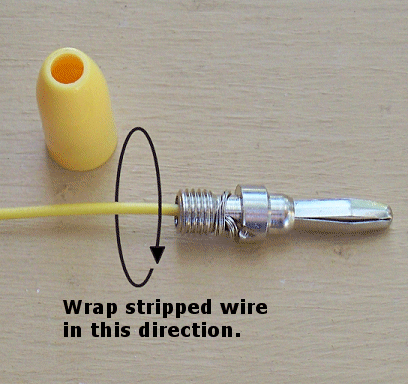 |
| The finished product. You should be able to tug on the wire and it should feel solid and not come out of the jack. | 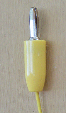 |
Wire Front Panel
Wire the front panel components together as shown in the wiring diagram. Carefully check your work as most mistakes happen in panel wiring. It is a good idea to print out the panel wiring diagram and check off the wires in the diagram as you install and solder them. For connections that will also connect to the PC board it is a good idea to temporarily tack solder the wire to the terminal leaving room for the wire that will also run to the PCB. Then when installing the panel to PCB wires apply more solder to the tacked connections to make them secure.Wire Panel to PC Board
Wire the circuit points marked on the front panel diagram to the corresponding circuit points on the PC board using stranded 22 to 24 AWG hook up wire. Try to keep the wiring as neat as possible and use care while soldering. Shiny joints earn you points - I just made that up.Turn Power Switch Off - Attach Battery
Insert a battery into the battery snap making sure to observe polarity. Even touching the battery terminals to the battery snap in the incorrect polarity can play havoc with your circuit if the power is on. Always have the power switch off when attaching the battery.Turn Power On
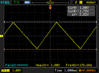
Turn the power on and monitor the output with an amplifier or oscilloscope. You should see the triangle and square waves as soon as you power the unit. They should be about 3 to 3.5 volts peak to peak when the output level is turned fully clockwise. You can use the output level pot to adjust the level as needed for use. You will need to adjust the sine wave trim pots in order to obtain a nice low distortion sine wave.Sine Wave Adjustment
- Adjust 100K trim pot R16 so that the top an bottom of the sine waveform have the typical sinusoidal curve. You don't want the wave to appear too flattened at the top or the bottom or too triangular. Adjust R16 until the sine wave looks as sinusoidal as possible.
- Use 100K trim pot R24 to adjust the top to bottom symmetry of the sine wave-shape.
- Use 100K trim pot R17 to adjust the amplitude of the sine wave-shape to about 3.5V peak to peak.
After trimming your sine wave should look like this.
Trouble Shoot As Necessary
Any time you turn on your project and it works first time... give yourself a nice pat on the back. Otherwise... You'll have some trouble shooting to do. Panel wiring is often a source of errors but there are a myriad of possible causes. Here are some tips I've put together over the years because as you can imagine I have done my fair share of trouble shooting. Trouble Shooting Tips...I hope you enjoy building this project and that it gives you years of service. As always... keep imagining, keep inventing, stay ingenious!
Kit Notes
Switches
The switches in this circuit are switching very low currents so they do not need high voltage or current ratings. Typical miniature toggle switch ratings are 1 to 5 amps at 115VAC which is way more than they will ever see in this circuit but that's what they make. Buy the cheapest switches you can because they will work fine. Of course if your last name happens to be Gates, Buffett, or Ellison you can buy gold plated toggle switches if you like since as long as they are the correct type (SPST (SPDT will also work as SPST)) they will all work.
More information
- Tell me something about switches?
- Reading Resistor Values
- What is a capacitor and what do the numbers on the capacitor mean?
Front Panel LED Mounting
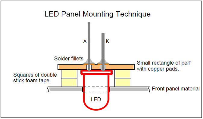
To mount the LED to the front panel I trim a small piece of pre-drilled perf board with copper pads into a small rectangle. The idea is to have perf board "ears" on either side of the LED after it is soldered to the small rectangle of perf board. I then cut double sided foam tape (the stuff that sticks forever) into small squares that I apply to the perf board on both sides of the LED (on the perfboard "ears"). I use a double stack of the foam tape so that the LED sticks through the panel less (you could go three layers if you want). I then push the LED through the panel and the double stick tape holds it in place. I leave the LED leads long so I can solder to them. If you trim them prior to wiring the panel to the PCB BE SURE TO LEAVE THE ANODE LEAD LONGER THAN THE KATHODE so you can tell them apart. I usually trim them when the intra-panel wiring is done.
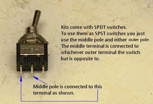
Kits come with SPDT switches which work perfectly as SPST
I send all Single Pole Double Throw Switches in kits because they also serve perfectly as SPST switches. As you can see in this image the switch has three terminals. The middle terminal is common and is connected to either of the outer terminals depending on the position of the switch bat. The terminal that is opposite of the way the switch bat leans is the terminal in contact with the middle terminal. Either outer terminal can be used.
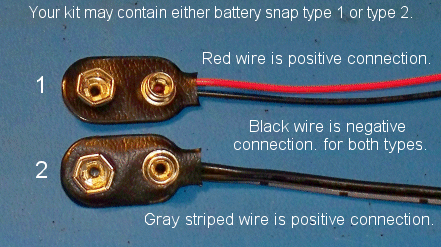
Battery Snaps
We ship two types of battery snap. One has red and black wire (type 1) and one has two black wires with one of them imprinted with a white broken stripe (type 2). With the red and black type the red is the positive connection. With the two black wire type the one imprinted with a white broken stripe is the positive connection.
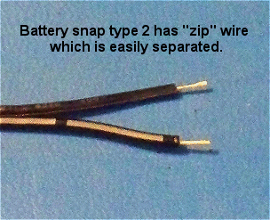
The type 2 snap (two black wire) has "zip" wire which can be separated easily by simply pulling the two wires apart near the stripped end.
Type 1 and 2 battery snaps. |
Type 2 zip wire separated. |
|---|---|
 |
 |
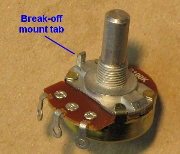
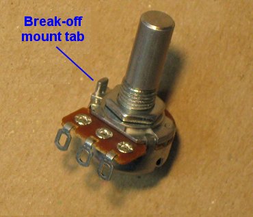
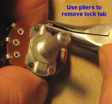
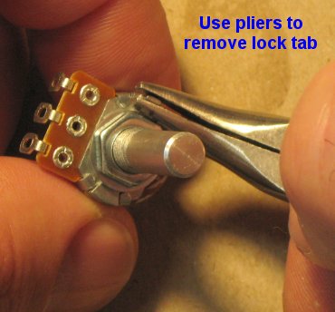
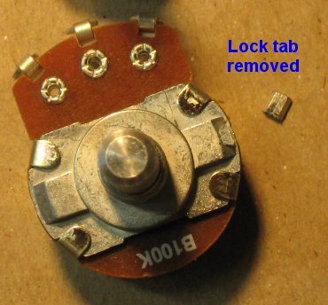
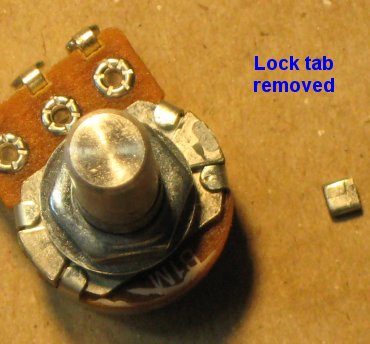
How To Remove Break-off Lock Tabs From Your Potentiometers
If your pots have little tabs on them you will need to remove them so that you can mount them to your faceplate. It is really easy to do. Carefully snap off the little tab near the pot body and voila it's done. Some kits come with larger pots and some kits come with smaller pots. The smaller pots are at times more expensive than the larger pots. They're all good quality pots and they all work the same way.
Regular Sized Pots |
Smaller Sized Pots |
|---|---|
| This is the break-off lock tab which can be used to keep the pot from turning when you turn the pot shaft but tightening the mounting nut works just fine. If you have the wherewithal to drill little holes for these pesky things... be my guest. If not... read on. | |
 |
 |
| Using pliers, grasp the tab as low on it as you can and then gently twist the pliers outward. I told you it was easy. | |
 |
 |
| The little broken off tabs look like this. Now you can mount your pot without the little tab getting in the way. | |
 |
 |