Ray Wilson authored this content while he was actively running MFOS as the founder and resident genius.
We retain the content because it reflects a valuable point of view representing that time and place.
Article by Ray Wilson
The MFOS Control Voltage And Gate Distributor is a great addition for your modular system. It is an excellent way to expand the outputs of a MIDI to CV convertor. Mine is indispensable since my MIDI to CV convertor only has one CV and one gate output. Also it allows you to add zipperless analog portamento (glide) to your MIDI to CV convertor's CV output.
I implemented this circuit on 3 of the Swiss OpAmp Knife PC boards to illustrate how to use them and how useful they can be.
The Control Voltage And Gate Distributor is useful for buffering the CV and gate output of a keyboard or a MIDI to CV convertor. It provides 5 gate outputs and 5 CV outputs two of which have portamento control. The CV inputs from the banana jack, quarter inch jack and coarse and fine offset voltage controls are fed into an inverting summer U1-D via R1 100K 1% resistor, R2 100K 1% resistor, R5 200K 1% resistor, and R8 2M 1% resistor respectively. U1-D's feedback resistor R9 100K 1% resistor provides a gain of -1 for control voltages fed in from the jacks and a gain of -.5 and -.05 for the coarse and fine control input resistors respectively. The output of U1-D is re-inverted by op amp U1-C whose gain is -1 so that the input voltage matches the sign of the output voltage. I selected R1, R2 and R9 so that they matched as closely as possible to insure a gain of -1 from U1-D for control voltage applied to the input. I also selected R6 and R7 to match as closely as possible to insure a gain of -1 from U1-C so that the control voltage applied to the input is faithfully reproduced. The output of U1-C feeds low pass filter R3, C1, and R4 which is intended to eliminate any small glitches on the input. The non-inverting inputs of U1-A, U1-B, U2-D and U2-C are fed from the low pass filtered output of U1-C. CV-Out 1, CV-Out 2 and CV-Out 3 are driven by non-inverting buffers U1-B, U1-A, and U2-D respectively. U2-C is used to drive the non-inverting inputs of U2-B and U2-A via the portamento circuits. R14 20 ohm resistor sets the minimum portamento time for CV-Out 4 while R15 1M log taper pot allows adjustment of CV-Out 4's portamento time. R14 in series with R15 determine how fast C3 charges and discharges as the control voltage changes. R21 20 ohm resistor sets the minimum portamento time for CV-Out 5 while R22 1M log taper pot allows adjustment of CV-Out 5's portamento time. R21 in series with R22 determine how fast C4 charges and discharges as the control voltage changes. 9.1V zener diodes Z1 and Z2 and associated components R26, C5 and R27, C6 are used to set the voltage applied to the ends of R10 100K linear taper pot and R11 100K linear taper pot so that changes in supply voltage from +/-12V to +/-15V will not affect the range of the controls. These pots are used to adjust the offset voltage of the Control Voltage Distributor portion of the circuit. When you adjust these pots ALL of the output control voltages are offset together.
The gate buffer circuitry consists of a non-inverting comparator (U3-D and associated components) and the non-inverting buffers U3-C, U3-B, and U3-A which drive the gate jacks. The comparator has a bit of hysteresis which reduces susceptibility to noise on the input. R28 100K 5% resistor holds the input at ground while not connected to anything. When the gate input connected to the non-inverting input of U3-D via R16 10K 5% resistor goes above about 1.2V the output of U3-D goes from about -10.5V to about +10.5V. All of the non-inverting followers connected to the output of U3-D follow this voltage. The diodes on the outputs of the non-inverting buffer op amps block the negative voltage and pass the positive excursion of the comparator to the outputs to be dropped on the 20K resistors connected to the cathodes of the diodes. Since the gate input of most circuitry ranges around 10K impedance the outputs can drive two gate outputs easily. Thus two of the non-inverting buffers drive two gate outputs. LED1 is driven by the output of U3-D and glows whenever the gate input is high (above about 1.2 volts).
Control Voltage And Gate Distributor Schematic

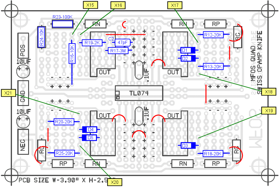
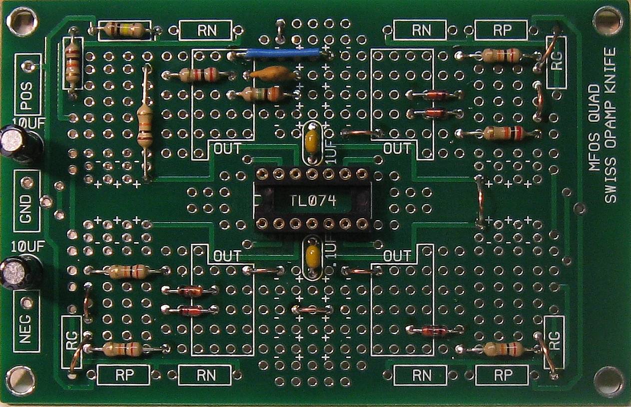
Control Voltage And Gate Distributor Board Details
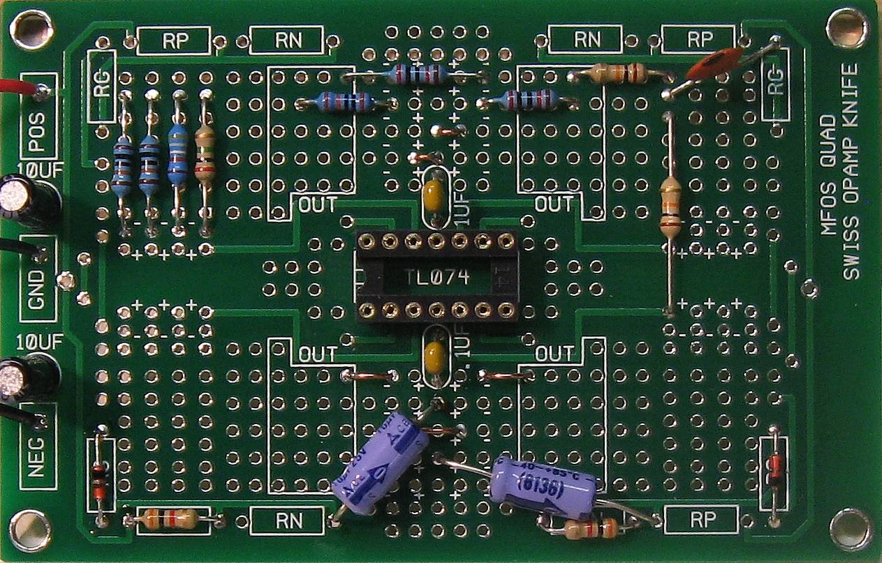
Control Voltage And Gate Distributor Board #1
Board 1 contains the control voltage summer, two of the control voltage output drivers (for CV-Out 1 and CV-Out 2) and the zener diode circuitry that supplies the coarse and fine voltage offset controls.
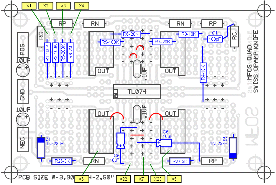
The careful observer will note that I did not have a 2M 1% metal film resistor. I have since replaced it with two 1M 1% in series. I also decided to change R5 to 200K 1% from the first value I tried on the bench (499K 1%) to give the Coarse offset more range.
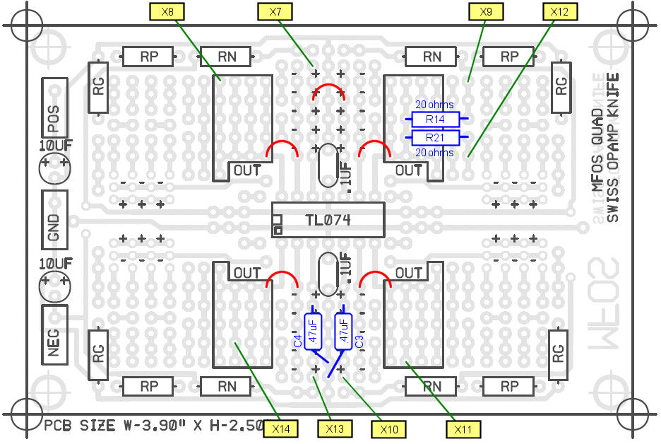
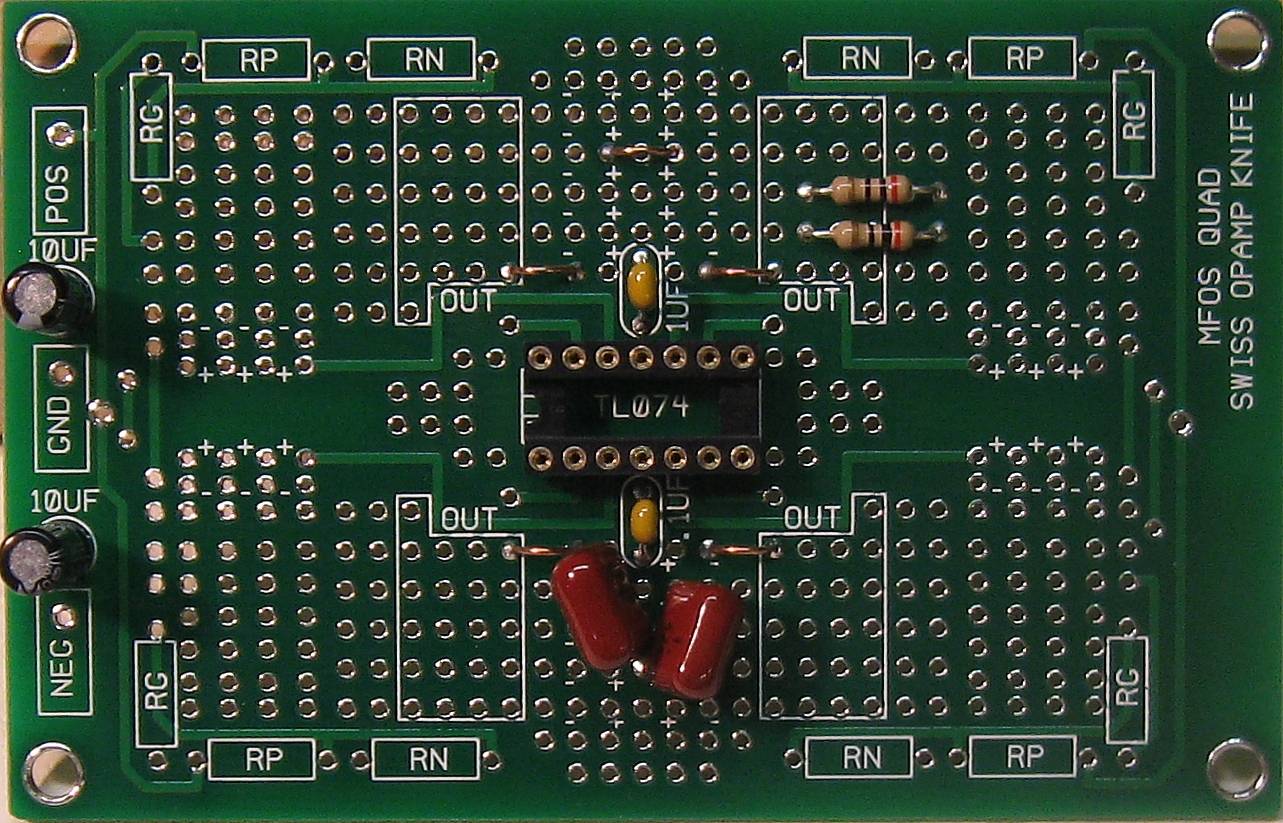
Control Voltage And Gate Distributor Board #2
Board 2 contains the circuitry for the CV-Out 3 buffer and the portamento controls in front of CV-Out 4 and CV-Out 5.
Control Voltage And Gate Distributor Board #3
Board 3 contains the gate comparator and gate drivers.
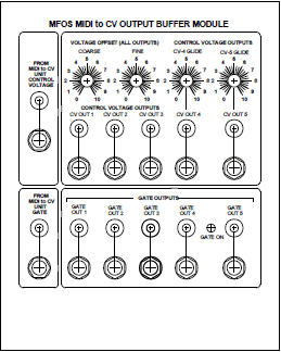
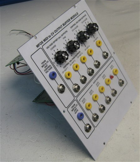
Control Voltage And Gate Distributor Panel
As usual this is just to illustrate one way to do this. As we all know there are many many... many.I also added a banana jack everywhere there is a phone jack so I can interface with my modular and my ULTIMATE.
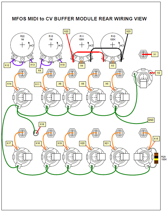
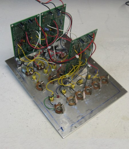
Control Voltage And Gate Distributor Panel Wiring
This corresponds with the suggested front panel layout but could probably be made much smaller.NOTE: R28 is mounted on the panel across the gate input jack.
I also added a banana jack everywhere there is a phone jack so I can interface with my modular and my ULTIMATE.
Notice that the CV inputs are actually separated and feed separate inputs whereas the gate input is just shorted to the banana jack.
Control Voltage And Gate Distributor Prototype
 |
 |
Micro Sample & Hold Project Parts List
Control Voltage And Gate Distributor Parts List
| Qty. | Description | Value | Designators |
|---|---|---|---|
| 3 | TL074 Quad Op Amp | TL074 | U1, U2, U3 |
| 5 | Diode 1N914 | 1N914 | D1, D2, D3, D4, D5 |
| 2 | 1N5239B 9.1V Zener Diode | 1N5239B | Z1, Z2 |
| 1 | General Purpose LED | LED | LED1 |
| 2 | Linear Taper Potentiometer | 100K | R10, R11 |
| 2 | Log Taper Potentiometer | 1M | R15, R22 |
| 3 | Metal Film Resistor 1/4 Watt 1% | 100K | R1, R2, R9 |
| 1 | Metal Film Resistor 1/4 Watt 1% | 200K | R5 |
| 2 | Metal Film Resistor 1/4 Watt 1% | 20K | R6, R7 |
| 1 | Metal Film Resistor 1/4 Watt 1% | 2M | R8 |
| 2 | Resistor 1/4 Watt 5% | 100K | R23, R28 |
| 4 | Resistor 1/4 Watt 5% | 10K | R3, R4, R16, R24 |
| 2 | Resistor 1/4 Watt 5% | 20 ohms | R14, R21 |
| 5 | Resistor 1/4 Watt 5% | 20K | R12, R13, R18, R20, R25 |
| 1 | Resistor 1/4 Watt 5% | 2K | R19 |
| 2 | Resistor 1/4 Watt 5% | 3K | R26, R27 |
| 1 | Resistor 1/4 Watt 5% | 3M | R17 |
| 2 | Capacitor Ceramic | .47uF | C3, C4 |
| 1 | Capacitor Ceramic | 100pF | C1 |
| 1 | Capacitor Ceramic | 47pF | C2 |
| 2 | Capacitor Electrolytic | 10uF | C5, C6 |
| 12 | Jack 1/4" 2 Terminal | . | |
| 12 | Banana Jack | . |