Ray Wilson authored this content while he was actively running MFOS as the founder and resident genius.
We retain the content because it reflects a valuable point of view representing that time and place.
Article by Ray Wilson
Features
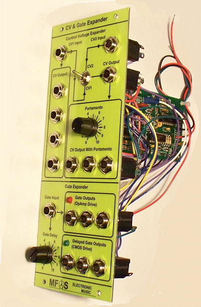
IntroductionOnce you start building up your modular you quickly learn that you need a lot of CV outputs to drive all of those VCOs, VCAs and VCFs. Additionally you never seem to have enough gates to drive all of the envelope generators, sequencers, and other modules that require them. That's where the MFOS CV and Gate Expander comes in. One CV input can drive 8 buffered CV outputs or two CV inputs can each drive four buffered CV outputs. Three of the CV outputs have portamento (glide). The gate input can drive 6 buffered gate outputs. Three of the gate outputs are op-amp drive and three of them are CMOS drive. The CV output is zener limited to provide protection from over-voltage. The gate output voltage levels are all customizable.
|
|
Schematics
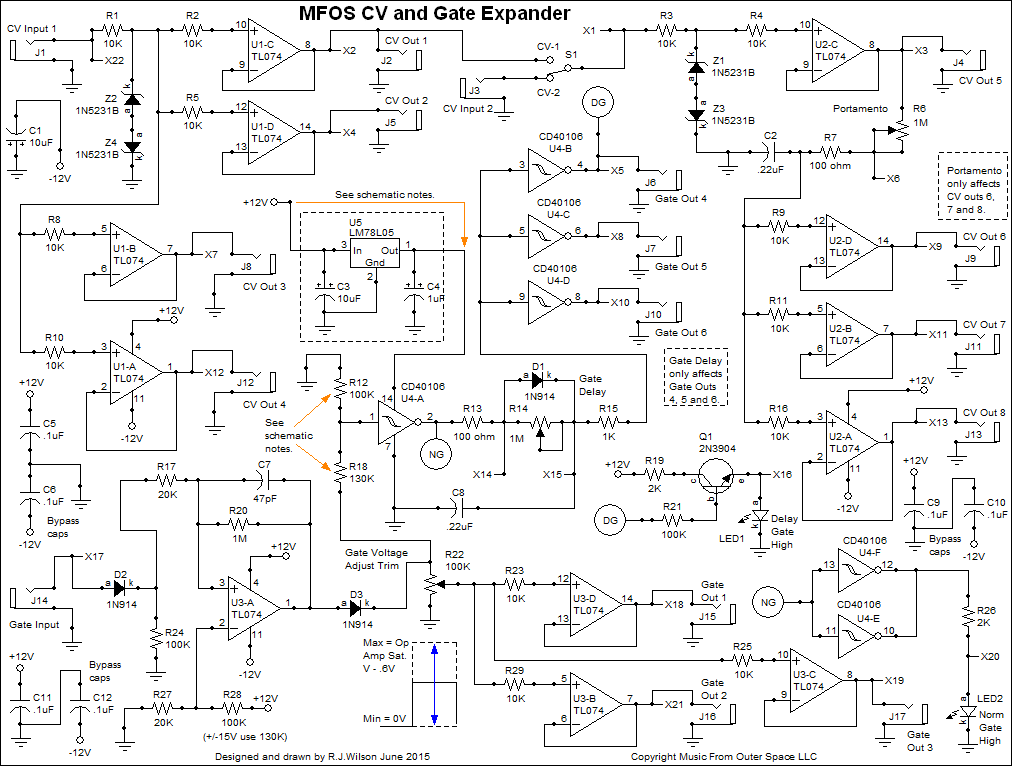
Schematic Page 1
View as PDFThis is a fairly straightforward circuit. Control voltage applied to CV Input 1 (J1) is routed to the non-inverting inputs of U1-A,B,C, and D. All four op amps have the inverting input tied to the output in order to provide a gain of one. Voltage applied at the jack causes current to flow through R1 (10K resistor) and through the 10K resistors R2, R5, R8 and R10 which are each connected to the non-inverting input of the four op amps U1-C, U1-D, U1-B, U1-A respectively. The back to back zener diodes at the junction of R1, R2, R5, R8 and R10 will only conduct if the voltage applied at the CV input jack is above the zener breakdown plus one diode drop. I nominally suggest 5V zeners but if your synth can only handle a maximum of +/-5V I suggest you go with 4V zeners which would conduct at +/-4.6V thus providing a small safety margin. You can tailor the zener voltage for your needs you don't have to use the 5V zeners I suggest. Of course the zener voltage must be less than the saturation voltage of the op amp outputs but you could use zeners from +/-3V up to +/-10V. I used 10V zeners in my boards since my synth uses higher voltage levels.
When the CV input voltage goes above the zener voltage plus one diode drop in either the positive of the negative direction one of the zener's will conduct and clamp the voltage to either +5.6V or -5.6V.
The outputs of U1-C, U1-D, U1-B and U1-A are connected to the output jacks J2, J5, J8, and J12 respectively.
Switch S1 is used to route either CV Input 2, via it's input jack or or the output of U1-C (which is buffering CV Input 1) to the non-inverting inputs of U2-C, U2-D, U2-B, and U2-A. Again the resistor and zener scheme (R3, Z1 and Z3) is used to limit the voltage fed to the op amp buffers. The output of U2-C feeds the portamento network which allows the user to add portamento (or glide) to the outputs of U2-D, U2-B, and U2-A. The output of U2-C charges and discharges capacitor C2 (.22uF film or ceramic capacitor) via R6 Portamento adjust pot and R7 100 ohm current limiter. The slewed voltage developed on C2 is fed via R9, R11, and R16 to the non-inverting inputs of U2-D, U2-B, and U2-A. Each of these op amps has its inverting input tied to its output resulting in a gain of one for each of them.
The input impedance of the TL074 is so high that the 10K resistors in the path to the non-inverting inputs has a negligible effect. The buffered output CV voltage(s) will follow the input very faithfully. Bear in mind that the op amps do have a small positive or negative offset voltage. Thus if you feed in 1.000 volts at the input you may see 1.005 volts or .995 volts on the output. If you then feed in 2.000 volts you should see 2.005 volts or 1.995 volts. The gross 1V change in voltage will be there with the op-amp's offset adding or subtracting as described.
The gate input is connected to a comparator circuit so that gate voltage of from 2.5V up to circuit V+ can be accepted at the input. Gate voltage applied to the input is fed via D2 (1N914) and dropped on 100K resistor R24. The voltage dropped on R24 is presented to U3-A's non-inverting input via 20K resistor R17. When the voltage at the non-inverting input rises above the 2V threshold voltage on the inverting input set by R27 (20K to ground) and R28 (100K to +V) the op amps output shoots high. R20 (1M resistor) provides a bit of hysteresis to the circuit to prevent output chatter during low-to-high or high-to-low output transitions. Capacitor C7 (47pF) gives a tiny kick of current to the non-inverting input which is always in the direction the output is heading which speeds up the comparator's transitions. The output of U3-A goes low again when the input voltage drops below the threshold voltage. The high excursion of U3-A's output is fed via D3 (1N914 diode) and dropped on R22 100K trim pot to ground. The wiper of trim pot R22 is fed (via resistors R23, R29, and R25) to the non-inverting inputs of U3-D, U3-B and U3-C respectively.
Trim pot R22 is used to adjust the voltage level of Gate Outs 1, 2 and 3. As you insert a gate signal into the unit, observe Gate Out 1 as you adjust trimmer R22 until the gate is at the desired amplitude. LED2 will illuminate when the input gate signal is high and be off when the input gate signal is low. U4-A's output, when low, drives the outputs of inverters U4-F and U4-E high. The outputs of inverters U4-F and U4-E are connected to provide greater LED current drive via R26 to LED2.
Important
Now we come to the CMOS drive gate outputs. If you are using a +/-12V supply or even a +/-15V supply and you need to limit the output voltage of the CMOS drive gates to a lower voltage (5V or 9V) you need to install the low power voltage regulator U5 and resistors R12 and R18. Low power regulator U5 is driven by the board's positive supply voltage and steps down the voltage powering U4 (Hex Schmitt Trigger Inverter). Resistors R12 and R18 are used to attenuate the saturated output voltage of U3-A to the output voltage level of the low power voltage regulator used to power U4. Since the input to U4-A is very high impedance the attenuation network can use high value resistors to reduce current drain. The resistors shown will attenuate the op amp's output voltage to accommodate using the 5V low power regulator shown. Since the output of U3-A in saturation is about 11V (on a +/-12V supply) the resistors shown will attenuate the voltage to about 4.78 volts which is plenty above the Schmitt input inverter's voltage threshold of about 3.33 volts.
If you don't need to attenuate your gate levels you can bypass the regulator with a wire jumper (shown in the PC drawing below), install a wire jumper in place of R18 and eliminate R12.
When the output of main gate buffer comparator U3-A goes high the output of U4-A (Schmitt Trigger Inverter) goes low. The low level on the output of U4-A discharges C8 (.22uF film or ceramic capacitor) via 100 ohm current limiting resistor R13 and 1M gate delay potentiometer R14. When C22 discharges below the threshold level of gates U4-B, U4-C and U4-D their respective outputs go high and appear on jacks J6, J7, and J10. R14 can be adjusted to insert a delay between the time the input gate goes high and the CMOS drive gates go high. This delay can be adjusted between 1mS to approximately 1.8 seconds. Diode D1 rapidly charges C8 when the output of U4-A returns high as the output of U3-A goes low in response to the gate input returning low. If the input gate is removed before the delayed gate goes high it will not go high. Additionally the delayed gate will return low synchronous with the gate input going low. LED1 will illuminate when the delayed gate goes high and be off when the input gate signal is low. Current from the output of U4-B, when its output is high drives transistor Q1's base via 100K base current limiter R21 and turns it on. Current flows from +12V via R19 and the transistor's collector and emitter and drives LED1. When point DG is low the transistor turns off and the LED goes off.
PC Board Information
If Using Full Supply Voltage For Gate Output
If you plan to use the power supply voltage for the output gate voltage you will not need to install U5 LM78L05 (or LM78L09), or R12 or R18. You will need to place a jumper wire from the input of the LM78L05 (pin 3) to it's output (pin 1). Another jumper wire must be used to bypass R18. Lastly, R12 need not be installed.
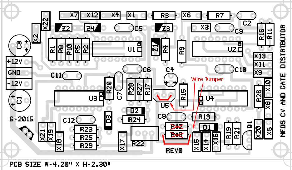
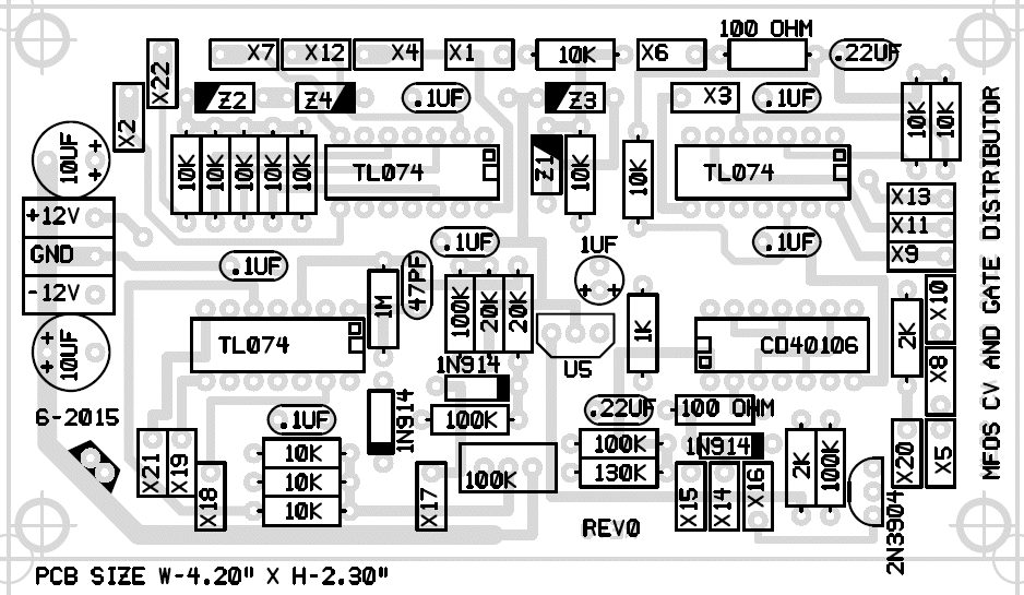
Parts Layout With Component Designators
This view is good for when you are trouble shooting.
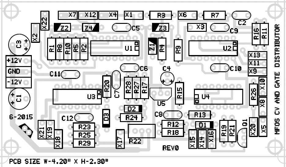
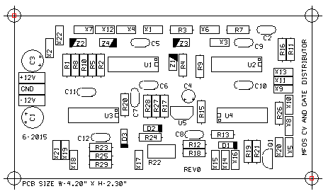
Parts Layout With Component Values
This view is good for when you are stuffing the PC board.
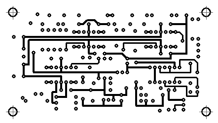
Top Copper
MFOS PCB Images are as viewed from the top of the PC Board. Keep that in mind when you are using the patterns with photo or copier processing.
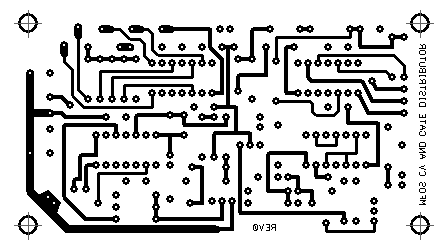
Bottom Copper
MFOS PCB Images are as viewed from the top of the PC Board. Keep that in mind when you are using the patterns with photo or copier processing.
Silk Screen
MFOS PCB Images are as viewed from the top of the PC Board. Keep that in mind when you are using the patterns with photo or copier processing.
Front Panel Information
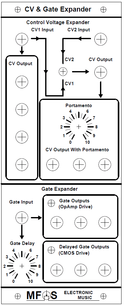
Suggested Front Panel Layout
View as PDFThe PDF is for a 8.75" x 3.5" format front panel.
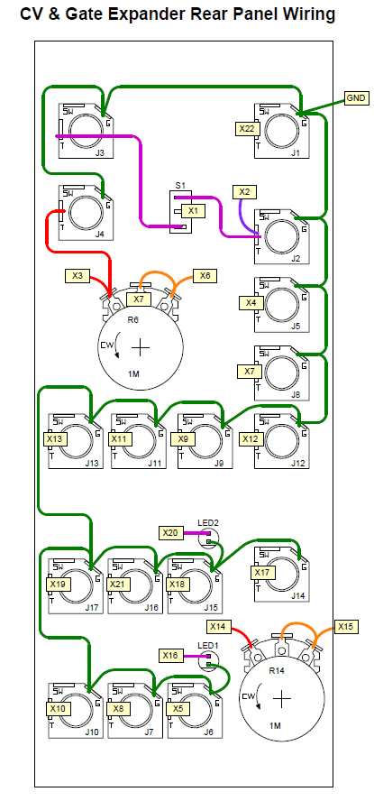
Suggested Front Panel Wiring Diagram
View as PDFI always use Amphenol style jacks these days because they have such a small footprint for a 1/4" jack. (Amphenol Part# ACJM-MVS-2S)
MFOS CV and Gate Expander Project Parts List
Component Notes
All cap voltages should be 25V or more. All resistors are 1/4W 5% (1% will work fine). MFOS PC boards use dual inline IC packages. MFOS PC boards usually use 5mm (0.2") cap lead spacing unless it is obvious from the board's legend that it should be larger or smaller. I often specify axial leads for any caps mounted on the front panel but you can use radial as well by adding some wire to the leads.
| Qty. | Description | Value | Designators |
|---|---|---|---|
| 1 | CD40106 | CD40106 | U4 |
| 1 | LM78L05 5V Voltage Regulator | LM78L05 | U5 |
| 3 | TL074 Quad Op Amp | TL074 | U1, U2, U3 |
| 1 | 2N3904 | 2N3904 | Q1 |
| 3 | Diode Switching | 1N914 | D1, D2, D3 |
| 4 | Diode Zener | 1N5231B | Z1, Z2, Z3, Z4 |
| 2 | LED | LED | LED1, LED2 |
| 2 | Potentiometer | 1M | R6, R14 |
| 1 | Potentiometer Trimmer | 100K | R22 |
| 2 | Resistor 1/4 Watt 5% | 100 ohm | R7, R13 |
| 4 | Resistor 1/4 Watt 5% | 100K | R12, R21, R24, R28 |
| 13 | Resistor 1/4 Watt 5% | 10K | R1, R2, R3, R4, R5, R8, R9, R10, R11, R16, R23, R25, R29 |
| 1 | Resistor 1/4 Watt 5% | 130K | R18 |
| 1 | Resistor 1/4 Watt 5% | 1K | R15 |
| 1 | Resistor 1/4 Watt 5% | 1M | R20 |
| 2 | Resistor 1/4 Watt 5% | 20K | R17, R27 |
| 2 | Resistor 1/4 Watt 5% | 2K | R19, R26 |
| 6 | Capacitor Ceramic | .1uF | C5, C6, C9, C10, C11, C12 |
| 2 | Capacitor Ceramic | .22uF | C2, C8 |
| 1 | Capacitor Ceramic | 47pF | C7 |
| 2 | Capacitor Tantalum Electrolytic | 10uF | C1, C3 |
| 1 | Capacitor Tantalum Electrolytic | 1uF | C4 |
| 1 | Switch SPDT | SPDT | S1 |
| 17 | Jack 1/4" 2 Terminal | . | J1, J2, J3, J4, J5, J6, J7, J8, J9, J10, J11, J12, J13, J14, J15, J16, J17 |