Ray Wilson authored this content while he was actively running MFOS as the founder and resident genius.
We retain the content because it reflects a valuable point of view representing that time and place.
Article by Ray Wilson
Features
Sample MP3sDelayed Modulation Sample 1 Delayed Modulation Sample 2 Delayed Modulation Sample 3 Delayed Modulation Sample 4
|
Introduction
|
If I had a nickle for every time I've patched up delayed modulation (also known as delayed vibrato)
I would be a very rich man... well maybe I'd at least be able to get a coffee at Starbucks.
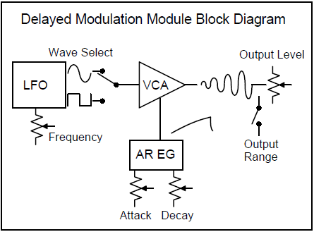
Anyway... this module includes an Attack Release envelope generator, Low Frequency Oscillator with square and sine waveforms, and a Voltage Controlled Amplifier. These separate elements are connected in the classic delayed modulation patch such that the LFO is fed to the input of the VCA and the AR generator is connected to the VCA's control input. When you apply a gate to the circuit the AR generator is gated on and the VCA responds to the applied envelope and the LFO comes through the VCA. You use the output of the module to modulate other voltage controlled modules. Since there is a complete AR generator built into the module you have some nice flexibility. You can do the usual slow increase in modulation or you can do the opposite meaning use a fast attack and slow delay so that the modulation starts high and goes low. I built this module into my keyboard controller and I love it Current drawn by this module is about 20 mA from +12V and 20 mA from -12V. |
|
Schematic Page 1
View as PDF
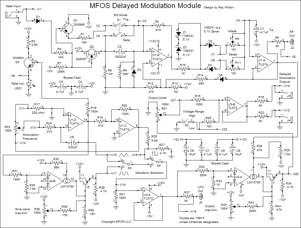
AR Generator
The AR generator is a great little design that only uses 2 op amps (half of a TL074). Typically in an AR generator you need a flip flop of some kind and in this circuit we use U1-B as our flip flop. An op amp as a flip flop? Read on...
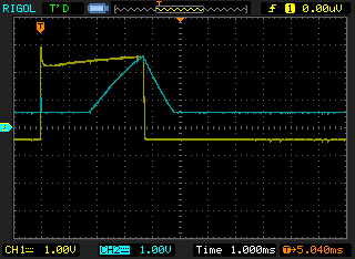
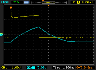
Switch S1 is in Trig position for this part of the circuit description. We use U1-B (1/4 TL074 quad JFET op amp) as a comparator and bias it so that it's output is normally low when the output of the AR generator (U1-A pin 1) is low. When U1-B's output is low (sitting at about -10.5V) R2 (91K resistor) pulls it's non-inverting input slightly below ground while R12 and R13 hold the inverting input slightly above ground. When a gate is applied (gate needs to step from ground to over 3V) D1 conducts and causes Q2 to turn on hard and drop +12V across R8 (1M resistor). The front edge of the voltage dropped on R8 propogates through C2 (.002uF ceramic capacitor) and is dropped on R9 (30K resistor) D3 insures that C2 does not cause large negative spikes on the non-inverting input of U1-B when the gate is removed. The positive pulse that is dropped on R9 causes the non-inverting input to go above the threshold on the inverting input and the output of U1-B shoots high. Now the feedback through R2 holds the non-inverting input above the voltage on the inverting input and the output of U1-A must go to the positive excursion of the AR envelope in order to bring the inverting input's voltage above that on the non-inverting input via D5 and R14 (39K resistor). In the left image the voltage on U1-B pin 6 appears delayed but that is just because D5 does not conduct until it is forward biased so the envelope at U1-A pin 1 has to go from below ground to above ground and then once the voltage is high enough to forward bias D5 it conducts.
Yellow = U1B pin 5, Blue = U1-B pin 6 After
|
Yellow = U1B pin 5, Blue = U1-A pin 1 After
|
Zener diodes Z1 and Z2 (1N5231 5.1V zener diodes) keep the voltage range of the resulting AR envelope within about + and - 5 volts (plus a diode drop). When U1-B's output is low (about -10.5V) Z2 conducts in the forward direction and Z1 zeners at about -5.1V. When U1-B's output is high (about +10.5V) Z1 conducts in the forward direction and Z2 zeners at about 5.1V. Current from U1-B charges C1 (4.7uF tantalum capacitor) via R10 (1K resistor), forward biased D2 and Attack pot R5 (1M audio taper pot). When the voltage on C1 gets high enough to bias the inverting input of U1-B (pin 6) above the voltage on the non-inverting input (pin 5) the output of U1-B shoots low and C1 is discharged via R10, forward biased D4, and Decay Pot R11 (1M audio taper pot). Voltage on C1 is buffered by U1-A whose output (pin 1) is the actual AR generator output. Attack and decay time adjustment ranges from a couple of milliseconds to about 8 seconds maximum.
When S1 is set to Gate mode and a gate is applied the AR generator goes high at the rate set by Attack pot R5 and then remains high as long as the gate is present. When the gate is removed Q1 turns on and jams the non-inverting input of U1-B negative and causes it's output to shoot low immediately which starts the decay cycle. Gated mode with a slow attack and fast decay are the typical settings for the classic delayed modulation patch.
LFO
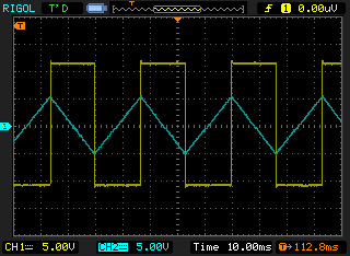
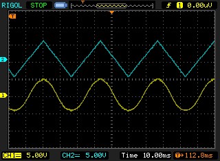
Op amps U1-D and U1-C are used to implement an LFO. It is the simple integrator followed by a comparator type oscillator. Essentially U1-D and U1-C chase one another. When U1-C's output is low (-10.5V) U1-D's output ramps up at a rate set by 100K Modulation Frequency pot R23. R23 is wired as a voltage divider and a portion of the voltage from the output of U1-C is fed via R24 (47K resistor) into the integrator formed by U1-D and feedback capacitor C5. The current through R24 is varied since I = E/R and the E is changed when we adjust R23. Thus we can change the rate at which the LFO oscillates by adjusting R23. The LFO goes from about 1.5 Hz at it's lowest setting to about 500 Hz at it's highest setting. The output of comparator U1-C is fed to resistive divider R25 and R27 to reduce the amplitude of the square wave to about +/-5V. The output of U1-D (triangular wave) is fed to the input of U2-B (LM13700 dual transconductance op amp). We use the non-linear distortion provided by overdriving the input to produce a nice approximation of a sine wave. Trimmer R38 is used to bias the sine wave so that it oscillates about ground (meaning goes equally high and low about the ground level). Adjust trimmer R38 until the sine wave oscillates evenly about ground. The sine wave appears at U2-B pin 9. The square wave and sine wave are wired to Waveform Selection switch S3 (SPDT toggle). The common terminal of S3 feeds the input of op amp buffer U3-A (1/2 TLO72 dual JFET op amp) whose output feeds the input of the VCA (U2-A and associated components).
Yellow = U1-C pin 8, Blue = U1-D pin 14.
|
Yellow = U2-B pin 9, Blue = U1-D pin 14.
|
VCA
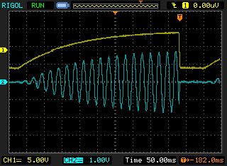
U2-A (1/2 LM13700 dual transconductance op amp) and associated components comprise the VCA. We hold U2-A bias pin 1 at a low level via R29 (7.5K resistor) and when the AR generator cycles the voltage from U1-A pin 1 drives current into the bias pin and the transconductance op amp passes the LFO signal through to it's output with an envelope determined by the setting of the AR generator. Trimmer R42 is used to bias the output of the VCA (U2-A pin 8) to 0V when no envelope is being applied. Turn the modulation range to high and the modulation amount pot all the way up and then measure the output (X10 or X12) with no gate applied. Adjust trimmer R42 until the output is as close to 0 volts as you can get it. The output of the VCA feeds Output Level pot R21 (100K linear pot) whose wiper feeds buffer amp U3-B via R15. when S2 is closed the amplitude of the output goes down by a factor of about 10. This is useful when your oscillator does not have a linear CV input as applying the output signal to an expo input without the attenuation may cause too much modulation for low level pitch modulation vibrato. U3-B's output feeds the two modulation output jacks via 3K isolation resistors.
Yellow = U1-A pin 1, Blue = U2-A pin 8.
Last but not least...
Although the schematic only uses the sine and square waves for modulation the board also has a connection point for the triangle waveform X15 (U1-D pin 14). Also the AR generator's output X8 and the LFO buffer's output X19 (U3-A pin 1) are both available as connection points on the PCB. I have not tried this circuit on +/-15V but I imagine a tweak or two may be in order. If you decide to use +/-15V and have any issues with the circuit please let me know and we will work through and fix them. There is absolutely nothing that prevents the circuit from working on +/-15V.
Drum Voice? Well... you have an LFO oscillator (1.5Hz to 500 Hz), VCA and AR generator which is all you really need. So if you use the circuit in this manner please let me know so others can benefit.
PC Board Information
PC Board Legends
View as PDF
PC Board Values
View as PDF
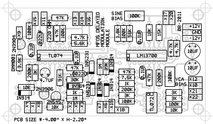
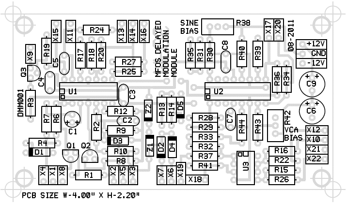
PC Board Populated View
(Newer boards have a bit more room for the VCA Bias trimmer but all boards are electrically identical)

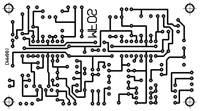
PC Board Bottom Copper
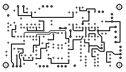
PC Board Top Copper
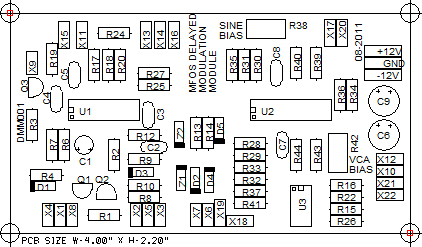
PC Board Silk
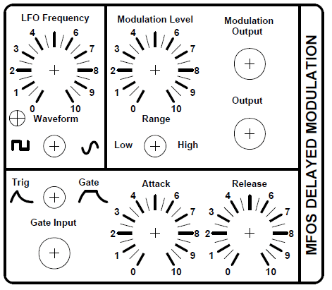
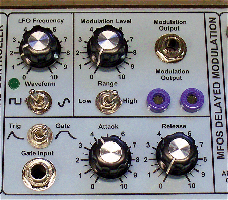
Suggested Panel Layout and Wiring
Suggested Panel Template
View as PDF
As you can see I added two banana jacks to the panel (instead of the second 1/4" jack) since my gear has both types of jacks.
|
|
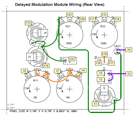
Suggested Panel Wiring
View as PDF
MFOS Delayed Modulation Module Project Parts List
!!!!!!! +/-15V System Users Read This !!!!!!!
Huge thanks to diyer Rémy Wasselin of France who uses +/-15V in his system. Rémy had some issues with this module powered with +/-15V as published and so he experimented and discovered several resistor value changes necessary to get the module functioning properly on +/-15V. Here are Rémy's suggested changes:
- R12 = 56K
- R14 = 22K
- R28 = 68K
- R32 = 100K
- R44 = 75K
| Qty. | Description | Value | Designators |
|---|---|---|---|
| 1 | LM13700 Dual gm OpAmp | LM13700 | U2 |
| 1 | TL072 Dual Op Amp | TL072 | U3 |
| 1 | TL074 Quad Op Amp | TL074 | U1 |
| 1 | 2N3904 NPN Transistor | 2N3904 | Q3 |
| 1 | 2N3906 PNP Transistor | 2N3906 | Q1 |
| 1 | 2N5457 N Channel JFET | 2N5457 | Q2 |
| 5 | 1N914 Diode | 1N914 | D1, D2, D3, D4, D5 |
| 2 | 1N5231 5.1V Zener Diode | 1N5231 | Z1, Z2 |
| 1 | General Purpose LED | Red LED | LED1 |
| 2 | Audio Taper Potentiometer | 1M | R5, R11 |
| 2 | Linear Taper Potentiometer | 100K | R21, R23 |
| 2 | Potentiometer Trimmer | 100K | R38, R42 |
| 1 | Resistor 1/4 Watt 5% | 5.6K | R25 |
| 1 | Resistor 1/4 Watt 5% | 56K | R30 |
| 1 | Resistor 1/4 Watt 5% | 7.5K | R29 |
| 1 | Resistor 1/4 Watt 5% | 91K | R2 |
| 3 | Resistor 1/4 Watt 5% | 10K | R1, R4, R26 |
| 1 | Resistor 1/4 Watt 5% | 15K | R39 |
| 1 | Resistor 1/4 Watt 5% | 1K | R10 |
| 1 | Resistor 1/4 Watt 5% | 1.8K | R35 |
| 5 | Resistor 1/4 Watt 5% | 100K | R15, R19, R20, R31, R41 |
| 1 | Resistor 1/4 Watt 5% | 18K | R40 |
| 1 | Resistor 1/4 Watt 5% | 1K | R33 |
| 2 | Resistor 1/4 Watt 5% | 1M | R8, R13 |
| 3 | Resistor 1/4 Watt 5% | 200K | R7, R32, R43 |
| 1 | Resistor 1/4 Watt 5% | 220 ohm | R17 |
| 1 | Resistor 1/4 Watt 5% | 3.9K | R3 |
| 1 | Resistor 1/4 Watt 5% | 30K | R9 |
| 1 | Resistor 1/4 Watt 5% | 39K | R14 |
| 4 | Resistor 1/4 Watt 5% | 3K | R6, R16, R22, R37 |
| 3 | Resistor 1/4 Watt 5% | 4.7K | R27, R34, R36 |
| 5 | Resistor 1/4 Watt 5% | 47K | R12, R18, R24, R28, R44 |
| 1 | Capacitor Ceramic | .0022uF | C2 |
| 1 | Capacitor Ceramic | .022uF | C5 |
| 4 | Capacitor Ceramic | 0.1uF | C3, C4, C7, C8 |
| 2 | Capacitor Electrolytic | 10uF | C6, C9 |
| 1 | Capacitor Tantalum | 4.7uF | C1 |
| 1 | Switch DPST | DPST | S1 |
| 1 | Switch SPDT | SPDT | S3 |
| 1 | Switch SPST | SPST | S2 |
| 3 | Jack 1/4" 2 Terminal | J1, J3, J4 |