Ray Wilson authored this content while he was actively running MFOS as the founder and resident genius.
We retain the content because it reflects a valuable point of view representing that time and place.
Article by Ray Wilson
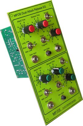
Dual Attack Release Envelope Generator Features
IntroductionEnvelope generators are a staple of any modular synth. Having lots of them gives you lots of options when it comes to VCA control, VCF control, delayed modulation, and AR modulation of anything else your heart desires. This dual AR generator is very cool and each EG features triggered, gated and repeat mode operation. When repeat is on (while in triggered mode) the EG continually goes through the attack and release cycles. In triggered mode the front edge of the gate (or a trigger signal) is used to trigger the circuit into operation. The attack cycle begins and completes and then the release cycle starts, the circuit can be re-triggered as soon as the release cycle begins. In gated mode when a gate is applied the attack cycle begins. If the gate is removed before the attack cycle completes (output attains maximum voltage of 10V) the release cycle begins. In gated mode, with repeat on, the EG repeats when the gate is low (when short times are used). In gated mode, with repeat on and the gate is held high the EG will go to and remain at the maximum output voltage (10V) until the gate is released at which time the EG will begin to repeat the AR cycles (when short times are used). Primarily repeat mode is designed to be used in triggered mode.
|
 |
Dual Attack Release Envelope Generator Schematic Page 1 PDF
| Designator | Value for +/-12V | Value for +/-15V |
|---|---|---|
| R1 | 20K | 100K |
| R2 | 100K | 200K |
| R24 | 100K | 130K |
| R22 | 47K | 100K |
| R23 | 3K | 5.1K |
| R26 | 9.1K | 16K |
| R27 | 33K | 27K |
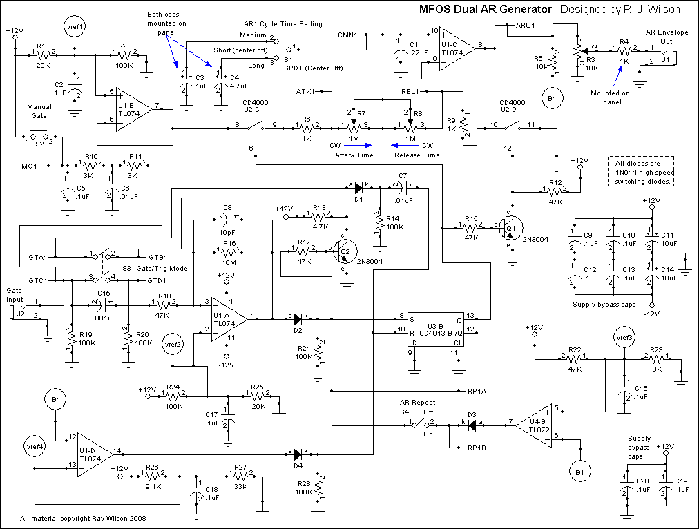
| The AR generator is controlled primarily by the state of D-Flip Flop U3-B. Normally
U3-B's "Q" output is low. In this state U2-C is off and U2-D is on allowing the timing cap C1 to be completely
discharged to ground.
Gated Mode In gated mode (switch S3 closed) when a gate signal is applied (voltage applied to the Gate Input which is greater than vref2 (about 2V)) the output of U1-A goes high (from -11V to +11V) the positive excursion of U1-A's output is fed via D2 and dropped across R21 which brings the "S" input of U3-B high which "sets" the Q output (pin 13) high (+12V). This high level turns on analog switch U2-C allowing the envelope timing cap C1 to begin charging to the voltage present on U1-B pin 7 via R6 (1K current limiter) and R7 (1M pot) Attack Time control. It also turns on Q2 so that the voltage on the collector of Q2 goes to ground. The voltage charging up on C1 is fed to U1-C non-inverting buffer which feeds the output level control and subsequently the output of the AR generator. This voltage is also fed via R5 (10K) to point "B1" which is connected to U1-D pin 12 and U4-B pin 5. The time that C1 takes to charge to the voltage on U1-B (approximately 10V) is the attack time. If the gate is held long enough the voltage on C1 will charge to the peak voltage (10V) and then remain there as long as the gate held. If the gate is released the output of U1-A's output goes to -11V. D2 blocks the negative excursion but the "S" input of U3-B and the base of Q2 see a ground level through R21. Thus Q2 turns off abruptly and its collector goes to +12V (via R13). The front edge of this square pulse is fed via D1 and C7 to the "R" pin of U3-B so that the flip flop is reset bringing the "Q" output low. U3-B's pin 13 going low turns off Q1 and thus +12V via R12 is fed to U2-D's control pin turning it on. C1 then discharges via R8 (1M pot) Release Time control and R9 (1K current limiter). The time it takes C1 to discharge to ground is the decay time. In gated mode the AR envelope follows the gate. If the gate is held the EG ramps up to max voltage at the rate set by the attack time and when the gate is released the EG ramps down to ground at the rate set by the Release Time. When the gate is removed prior to the EG output reaching the maximum output voltage (10V) the EG immediately enters the release state. The repeat function is primarily designed to be used in triggered mode. But in gated mode the repeat function will work while the gate is low and cease when the gate is high. Switch S1 "AR1 Cycle Timing Setting" is used to place additional capacitance in parallel with C1 thus increasing the AR times. The larger the capacitance in parallel with C1 the longer the AR times that can be achieved. Conversely the minimum attack and release times will be increased with either additional cap in parallel with C1. Triggered Mode In triggered mode (S3 open) the Ar generator will achieve the maximum output voltage whenever it is triggered to begin an AR cycle. In triggered mode it does not matter if a trigger or a gate signal is applied to begin the attack cycle. Only the front edge of either is presented to the input of U1-A via C15 (which is not shorted out when S3 is open). Thus only a pulse is applied to the "S" input of U3-B and the attack cycle begins (since U2-C is on allowing C1 to charge and U2-D is off). The output of U1-C (which is the buffered voltage appearing on C1) is fed via R5 to point B1 which is connected to the non-inverting input of comparator U1-D. When the voltage at B1 goes above the threshold of U1-D (vref4 appied to it's non-inverting input) U1-D pin 14 goes high and resets U3-B via D4 bringing U3-B's reset (pin 10) high. When U3-B is reset it's Q output goes low and the AR gen enters release mode and C1 discharges via analog switch U2-D, R9 (1K) and R8 (1M pot) Release Time Control. Repeat Mode (Used in conjunction with triggered mode) When S4 is on comparator U4-B triggers U3-B back into attack state when the release cycle discharges C1 to the level below the threshold of U4-B (vref3 approx .72V). Thus the Ar generator continually emits the AR envelope. The envelope timing can be changed using the Attack and Release time controls as well as the AR1 Cycle Timing Setting. Manual Gate Momentary pushbutton switch S2 applies +12 volts via a two pole filter (to reduce switch bounce) to the gate input. When pressed the AR generator is gated or triggered dependding on the currently set Gate/Trigger mode. |
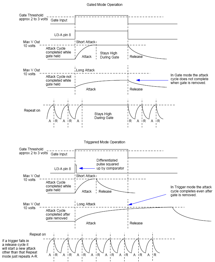
Dual Attack Release Envelope Generator Timing Diagram PDF
The second AR generator in the Dual AR generator works identically to the one described above.
Dual Attack Release Envelope Generator Schematic Page 2 PDF
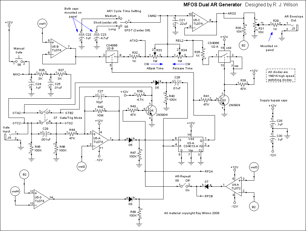
Page two shows the second AR generator. The circuit description is the same as for page one (with the exception of designators).
| Approx. Current Consumption | |
| +12V | 24 mA |
| -12V | 18 mA |
| +15V | 25 mA |
| -15V | 18.5 mA |
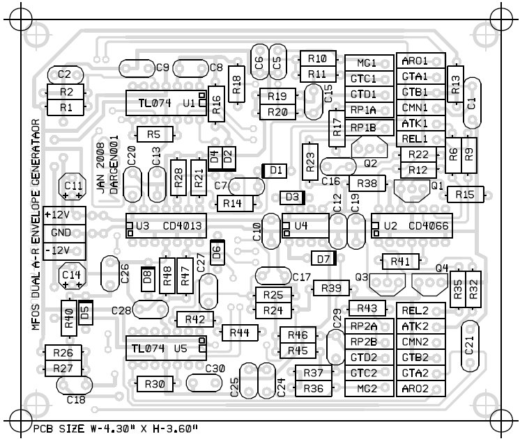
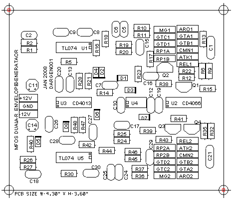
Dual Attack Release Envelope Generator PCB Parts Layout (Parts Side Shown) PDF
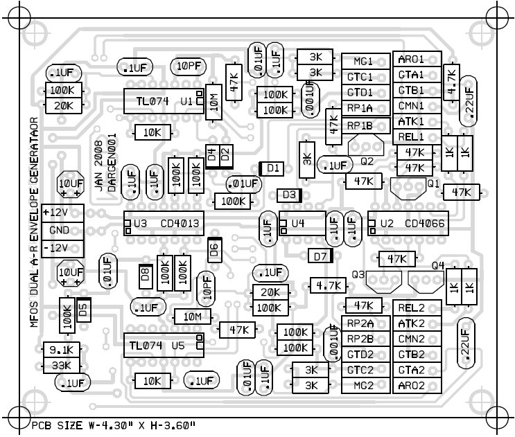
Dual Attack Release Envelope Generator PCB Parts Layout (Values Shown) PDF
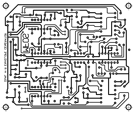
Dual Attack Release Envelope Generator PCB Bottom Copper (Parts Side Shown)
| This image needs to be scaled so that DIP pad centers are spaced 1/10" apart (and 3/10" apart for pins across from one another). Consult your graphics aware friend for how to do that if you need to. |
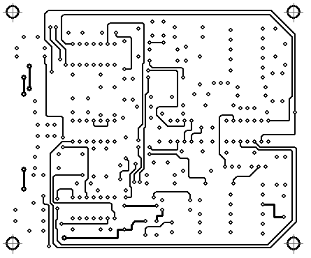
Dual Attack Release Envelope Generator PCB Top Copper (Parts Side Shown)
Dual Attack Release Envelope Generator PCB Silk Screen (Parts Side Shown)
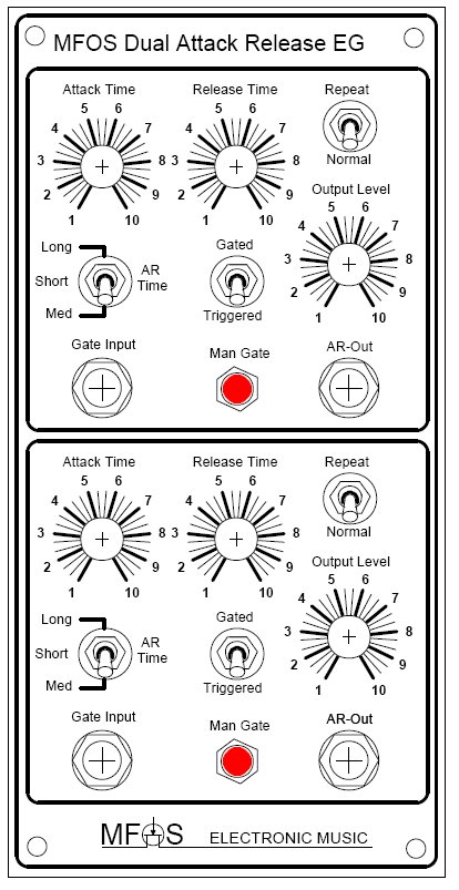
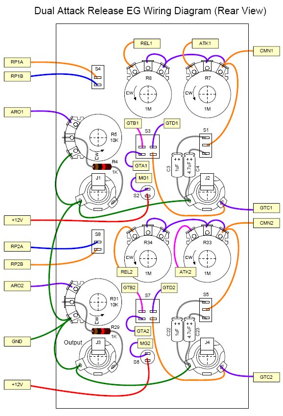
Dual Attack Release Envelope Generator Front Panel (PDF) Dual Attack Release Envelope Generator Panel Wiring PDF
| I recommend using an aluminum panel so that it can be attached to ground and thus ground all of the pot bodies. This is a recommended layout only and is here to correspond with the wiring view so people know how to wire the module. Feel free to do it the way and in the synth format you like. |
 |
 |
Dual Attack Release Envelope Generator Project Parts List
***Dual Inline Package (plastic or ceramic)
Dual AR Generator Project Parts List
| Qty. | Description | Value | Designators |
|---|---|---|---|
| 1 | CD4013 Dual D Flip Flop*** | CD4013 | U3 |
| 1 | TL072 Dual Op Amp*** | TL072 | U4 |
| 2 | TL074 Quad Op Amp(s)*** | TL074 | U1, U5 |
| 1 | CD4066*** | CD4066 | U2 |
| 8 | 1N914 Sw. Diode(s) | 1N914 (or 1N4148) | D4, D3, D2, D1, D8, D7, D6, D5 |
| 4 | 2N3904(s) | 2N3904 | Q1, Q2, Q3, Q4 |
| 2 | Capacitor Ceramic(s) | .001uF | C15, C29 |
| 4 | Capacitor Ceramic(s) | .01uF | C7, C6, C25, C26 |
| 14 | Capacitor Ceramic(s) | .1uF | C16, C17, C18, C2, C19, C20, C13, C12, C9, C10, C5, C30, C28, C24 |
| 2 | Capacitor Ceramic(s) | .22uF | C1, C21 |
| 2 | Capacitor Ceramic(s) | 10pF | C8, C27 |
| 2 | Capacitor Electrolytic(s) | 10uF | C14, C11 |
| 2 | Tantalum Electrolytic Cap(s) | 1uF | C3, C22 |
| 2 | Tantalum Electrolytic Cap(s) | 4.7uF | C4, C23 |
| 2 | Lin Potentiometer(s) | 10K | R3, R31 |
| 4 | Log Potentiometer(s) | 1M | R7, R8, R33, R34 |
| 12 | Resistor 1/4 Watt 1%(s) | 100K | R28, R21, R14, R19, R24, R2, R20, R48, R47, R45, R46, R40 |
| 2 | Resistor 1/4 Watt 1%(s) | 10K | R5, R30 |
| 2 | Resistor 1/4 Watt 1%(s) | 10M | R16, R42 |
| 6 | Resistor 1/4 Watt 1%(s) | 1K | R4, R6, R9, R29, R32, R35 |
| 2 | Resistor 1/4 Watt 1%(s) | 20K | R25, R1 |
| 1 | Resistor 1/4 Watt 1% | 33K | R27 |
| 5 | Resistor 1/4 Watt 1%(s) | 3K | R23, R10, R11, R36, R37 |
| 2 | Resistor 1/4 Watt 1%(s) | 4.7K | R13, R39 |
| 9 | Resistor 1/4 Watt 1%(s) | 47K | R12, R22, R15, R17, R18, R38, R41, R44, R43 |
| 1 | Resistor 1/4 Watt 1% | 9.1K | R26 |
| 2 | SPDT (Center Off) Switch(s) | SPDT | S1, S5 |
| 2 | SPST Momentary PB SW(s) | SPST | S2, S6 |
| 2 | SPST Switch(s) | SPST | S4, S8 |
| 2 | DPST Switch(s) | DPST | S3, S7 |
| 4 | Jack 1/4" 2 Terminal(s) | J1, J2, J3, J4 |
Miscellaneous
- (1) 1/16" thick Aluminum plate for mounting the pots and switches.
- Assorted hardware 1" 6-32 nuts and bolts, 1/2" #8 wood screws, etc
- Knobs for potentiometers, wire, solder and typical assorted electronics hand tools.
- Volt Meter and an Amplifier (or oscilloscope) for testing and enjoying.