Ray Wilson authored this content while he was actively running MFOS as the founder and resident genius.
We retain the content because it reflects a valuable point of view representing that time and place.
Article by Ray Wilson
This is an intermediate to advanced project and I do not recommend it as a first project if you are just getting started in synths or electronics. Only the circuit and some explanation are shown here. A lot of project building, troubleshooting and electronics experience is assumed. Additionally, electronic equipment ownership (scope, meters, etc.) is taken for granted. If you are interested in building this project please read the entire page before ordering PC boards to ensure that the information provided is thorough enough for you to complete the project successfully.
Introduction
I am finding that the ambient electronic music I am creating is requiring lots of cyclic voltage changes. Here is a circuit to pluck chaotic patterns from whatever waveform you choose to plug into the input.Circuit Description
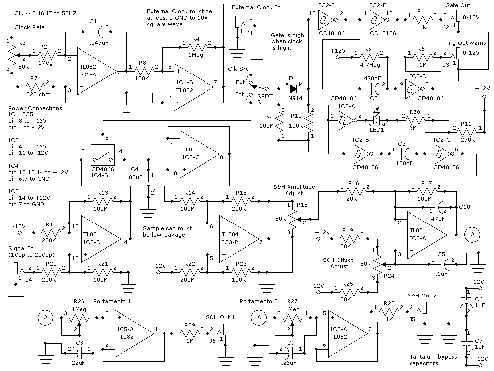
IC1-A and IC1-B make up a simple oscillator to provide the sample clock for this circuit. Theory of this oscillator's operation is described on the Super Simple Ramp/Sawtooth LFO page. IC2 and associated components are used to create the actual 0 to 12 volt sample pulse and trigger as well as the gate and LED driver circuit. When a clock (-12 to +12V internal, 0 to -12V external square wave) is applied to the anode of D1 the junction of D1's cathode and pin 2 of R10 goes from 0 to +12V. In turn IC2 pins 12, 2, and 4 all go low. The low going edge pulls pin 9 and pin 5 low momentarily (until the respective resistors to +12V pull the pins back up to 12V). This causes a momentry high pulse on the respective outputs (pins 8 and 6). The pulse at pin 6 is about 30uS wide and the pulse at pin 8 (the trigger output) is approximately 2.5 mS wide (See the CMOS Mickey Mouse Logic page). IC2 pin 10 simply follows the input at pin 13 (due to the double inversion). IC2-A's output goes low when the clock is high and thus sinks current and causes LED1 to go on and off as the clock signal goes high and low.The signal in is fed into IC3-D which is wired to have a gain of 1/2 and an offset of +6 volts. Thus its output always stays between 0 and 12 volts which is just what IC4-B likes. Applying voltages more negative than ground to pin 3 of IC4-B will forward bias its protection diodes and bad things will happen (high current will flow and poof IC4-B will go to chip heaven or chip hell depending on what kind of life it has led... and here the poor thing has been carousing with analog synthesizer components and I don't know how that is viewed in spiritual component circles, so be careful). OK the current sinking capability of IC3-D will really determine if it will blow or not and it might or might not. In any case I don't recommend applying voltages higher or lower than the circuit supply voltage.
IC4-B essentially connects pin 3 to pin 4 whenever the logic level at pin 5 is high. Since we are applying 30uS pulses to pin 5 it is only high long enough to allow C4 to charge (or discharge) to the voltage present at pin 3 (IC3-D's output). This sampled voltage is held (thus Sample and Hold) on C4 since IC3-C's input (pin 10) is ultra-high impedance (OK... resistance in this case) and the path back through pin 4 to pin 3 is essentially open because pin 5 is low for the great majority of the time. The output of IC3-C goes into IC3-B which is wired to have a gain of 2 and an offset of -6 volts (this gain and offset restore the signal to what we had at the Signal In input of the circuit). From pin 7 of IC3-B the signal is applied to R18 (voltage divider) where a portion of the signal is fed into IC3-A. Notice that IC3-A provides a gain of up to 5 (in conjunction with the setting of R18) so that you can boost smaller signals. Of course you can reduce large signals by turning R18 down as well. R24 allows you to offset the sampled and held voltage positively or negatively. IC3-A's output feeds two independent portamento circuits (and ultimately the outputs) for added versatility.
A small point, but worth mentioning. Often when you are working on a solderless breadboard with op-amps everything will work fine but when you finally lay out a board and install the components you may notice that op-amps (usually when gain is greater than 1) will oscillate at a very high frequency. This may manifest itself on your oscilloscope screen (when viewing the output of the op-amp) as fat horizontal looking lines despite your having turned the intensity of the beam down. Increase the vertical gain and turn the sweep up to the uS range and voila you will often find high frequency sinusoidal oscillation. To rid yourself of this evil you can do one of two things. 1) sacrifice a known good op-amp and throw its pins into a field where no rain has ever fallen... or 2) Apply a small capacitor in parallel with the feedback resistor of the offending op-amp. Something between 10 and 100 pF will do the trick. That is the function of C10 in the circuit. Why didn't it oscillate on the solderless breadboard? Because the solderless breadboard has pFs of capacitance between all of those hundreds of connection points.
Sample and Hold Circuit II
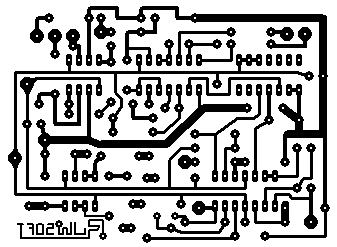
Sample and Hold Circuit II PCB Layout (Component Side View)
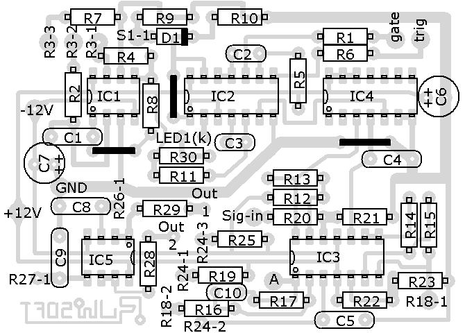
Sample and Hold Circuit II Parts Placement