Ray Wilson authored this content while he was actively running MFOS as the founder and resident genius.
We retain the content because it reflects a valuable point of view representing that time and place.
Article by Ray Wilson
This is an intermediate to advanced project and I do not recommend it as a first project if you are just getting started in synths or electronics. Only the circuit and some explanation are shown here. A lot of project building, troubleshooting and electronics experience is assumed. Additionally, electronic equipment ownership (scope, meters, etc.) is taken for granted. If you are interested in building this project please read the entire page before ordering PC boards to ensure that the information provided is thorough enough for you to complete the project successfully.
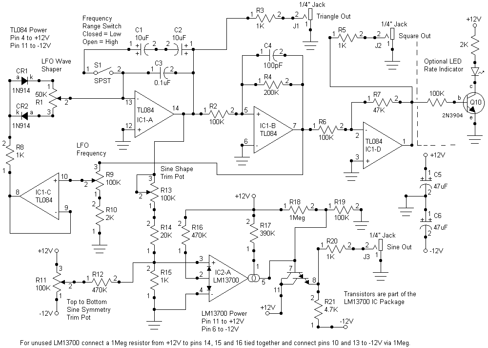
IntroductionThis is a cool little LFO for all of your modulation needs. It produces low frequency oscillations (as low as 1 cycle per minute to about 500 Hz) with output shapes of Sine, Triangle, Square, Pulse, Ramp, and Sawtooth waves (also Sine-ified (if that's a word) Ramp and Sawtooth waves). I would combine a couple of these with the Dual 4 Channel DC Mixer Circuit Schematic so you could adjust the output levels of the wave forms.Circuit DescriptionThe circuit works as follows: IC1-A is an integrator which is the heart of the oscillator. IC1-B is a comparator (with a lot of hysteresis) that is sensing the output of IC1-A. On power on, lets say that IC1-B is low (-12 volts) and R1 (LFO Wave Shaper) is at its center point. IC1-B's output is fed to pin 3 of R9 (100K frequency pot). R9 acts as an adjustable voltage divider and R10 (2K resistor) insures that the wiper (pin 2) of R9 is never completely grounded. IC1-C is a unity gain follower (whatever is on its input is seen at its output) and provides a low impedance source of voltage to push (or pull) current through R8 and CR1, CR2, and R1. If (pin 2) of R9 were completely grounded no current would flow through R8 and the LFO oscillation would stop. As it is, when the wiper (pin 2) of R9 is turned all the way toward R10 the oscillator is at its lowest frequency. This is because the voltage appearing on pin 8 of IC1-C determines the current that will flow through R8, CR2, and R1. Because IC1-A is an integrator all it needs is some current to flow into (or out of) its inverting input to cause the output to correspondingly fall or rise linearly. More current makes it rise or fall faster (thus increasing the LFO frequency). Now since we said we would start out considering IC1-B's output low then IC1-A's output will rise at a rate determined by the adjustment of R9. When IC1-A's output reaches about 6 volts (determined by the ratio of R2 to R4) IC1-B's output shoots high. C4 snaps up the rise and fall of IC1-B by pushing (or pulling) a quick spike of current to the non-inverting input (pin 5) of IC1-B when the output starts to shoot high or low. Once IC1-B's output is high (+12V), its output is sourcing (producing) 60 uA through R4 to the non-inverting input (pin 5) of IC1-B. In order to lower the voltage at pin 5 to below ground you need to sink (consume) a little more than 60 uA through R2 into the output of IC1-A. This happens when IC1-A's output ramps to slightly lower that -6 volts in response to IC1-B's output going high. At that point IC1-B's output goes low again and the cycle begins anew.R1 determines the ratio of charge to discharge current for integrator IC1-A and associated components. Current out of pin 8 of IC1-C is always sourced through CR1 and always sinked through CR2. R1 determines the sink to source ratio and thus the rise and fall rates of IC1-A's output. When R1 is adjusted to either end the current available for sourcing or sinking is limited only by R8 (1K resistor). When adjusted thus you will get a ramp (adjusted toward pin 1) or sawtooth (adjusted toward pin 3) shaped wave at the output of IC1-A. Centering R1 produces a triangle wave at pin 1 of IC1-A. IC1-D is used to attenuate the square/pulse wave to + and - 6 volts (to match the other output levels). The sine shaping circuitry uses the non-linear distortion characteristic that results from overdriving the input of a transconductance amplifer. We use one half of a LM13700 for this function. The 'Sine Shape' trim pot determines the amount of distortion (rounding of the top and bottom of the triangle wave) by adjusting the triangle wave voltage dropped across R15 1K resistor. The attenuated signal is fed into the non-inverting input (IC2-A pin 3) of the LM13700. The 'Top to Bottom Symmetry' trim pot is used to bias the non-inverting input (IC2-A pin 3) of the LM13700 up or down as necessary to produce equal rounding of the top and bottom portions of the distorted triangle wave. The LM13700's built in buffer amplifier (darlington transistor) is used to buffer the sine wave signal. C5 and C6, as typical, are used to stabilize the circuit's power supply. Pots R1 and R9 should be panel mounted. Switch S1 just switches in a larger capacitance to cause the integrator to take longer to charge and discharge. Frequencies of well below 0.1 Hz are easily obtainable. All outputs are protected from shorts to ground or other signals by 1K resistors. A board layout will be coming as soon as I finish my PC Board layout program. December 22, 2002 I improved the board layout a little and made it smaller and eliminated the overly thin traces. I also added a rate indication LED driver circuit. I am building a couple of these because I finally ran out of modulators. If there are any changes necessary I will post them but I have heard from others who have built the previous circuit board that it worked fine. Oh... and I made the boards using the film that you run through your laser printer and then iron on to the copper clad board. It took a little practice but in the end it worked. Wow! no darkroom needed. Good synthing... Ray Wilson December 24, 2002: Changed C4 from 100pF to 10pF. The circuit and board work fine.
|
Low Frequency Oscillator #1 Schematic
|
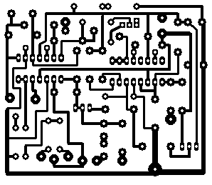
Low Frequency Oscillator #1 PC Board (Top View)
|
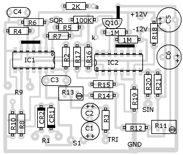
Low Frequency Oscillator #1 Parts Placement (Top View)
|
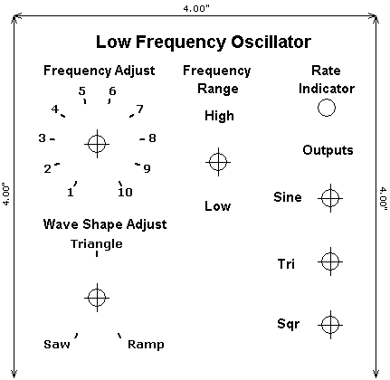
Suggested Panel Layout
|
Low Frequency Oscillator #1 Project Parts List
| Qty. | Description | Value | Designators |
|---|---|---|---|
| 3 | 1/4 Watt 1% Resistor(s) | 100K | R2, R6, R19 |
| 5 | 1/4 Watt 1% Resistor(s) | 1K | R3, R5, R8, R15, R20 |
| 3 | 1/4 Watt 1% Resistor | 1Meg | R18, (2 R's marked 1Meg) |
| 1 | 1/4 Watt 1% Resistor | 200K | R4 |
| 1 | 1/4 Watt 1% Resistor | 20K | R14 |
| 1 | 1/4 Watt 1% Resistor | 2K | R10 |
| 1 | 1/4 Watt 1% Resistor | 390K | R17 |
| 1 | 1/4 Watt 1% Resistor | 4.7K | R21 |
| 2 | 1/4 Watt 1% Resistor(s) | 470K | R12, R16 |
| 1 | 1/4 Watt 1% Resistor | 47K | R7 |
| 1 | Ceramic Capacitor | 0.1uF | C3 |
| 1 | Ceramic Capacitor | 100pF | C4 |
| 2 | Electrolytic Capacitor(s) | 10uF | C1, C2 |
| 2 | Electrolytic Capacitor(s) | 47uF | C5, C6 |
| 1 | LM13700 OP-Amp | LM13700 | IC2-A |
| 1 | Operational Amplifier | TL084 | IC1-D, IC1-A, IC1-B, IC1-C |
| 3 | Phone Jack(s) | 1/4" Jack | J1, J2, J3 |
| 1 | Potentiometer | 100K | R9 |
| 2 | Trim Pot(s) | 100K | R11, R13 |
| 1 | Potentiometer | 50K | R1 |
| 1 | SPST Switch | SPST | S1 |
| 2 | Silicon Diode(s) | 1N914 | CR1, CR2 |