Ray Wilson authored this content while he was actively running MFOS as the founder and resident genius.
We retain the content because it reflects a valuable point of view representing that time and place.
Article by Ray Wilson
|
|
Introduction
This phase shifter is designed around the phase shift cell found in several 1970s to 1980s units. It is not an exact copy of any of them but is modeled after them. It uses a transconductance amplifer to produce a voltage controlled variable phase shift. Mixing the phase delayed signal with the original produces notches in the resultant output.
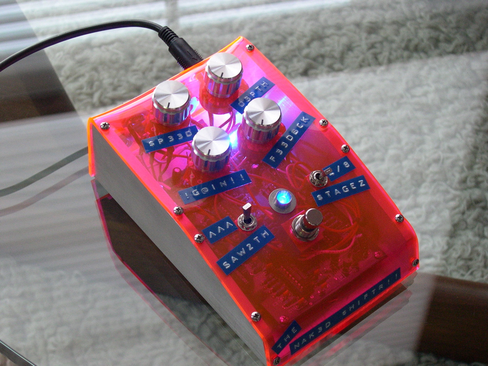
Alison Hughes' MFOS Phase Shifter
I just wanted to thank you for your awesome phase shifter circuit design - it sounds great! Everyone I have showed it to agrees that it's one of the best phase shifters they've ever heard. We especially like how extremely the parameters can be adjusted to make dramatic, watery sounding effects. I had this vision of putting it into a hot pink clear acrylic enclosure with an 80's punk rock aesthetic - large aluminum knobs and those old embossed labels. With help from a friend, I was able to create this crazy enclosure. We added some blue LEDs and it looks really cool in low light. My terrible rats nest of a wiring job makes it look more frankenstein- like with the LEDs lighting it from underneath. I gave it to my boyfriend as a birthday present and he uses it all the time in his studio!
See more photos at Alison's Flickr Site
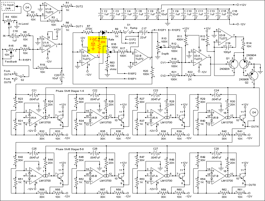
Eight Stage Phase Shifter Schematic Page 1 PDF
Kludge to Increase Output Level (If you want higher output levels do this...)
|
Increasing Output Levels
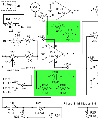
A diyer who had bought the Phase Shifter board was concerned that the output levels were too low and that increasing the input level was causing distortion. It is important not to over-drive the input (or things sound bad) so I came up with a fix. I increased the output level and kept the level going into the phase shift array the same as it was by splitting the feedback resistor around U1-A into a 10K (R19) and a 33K (R65) and by feeding the phase shifter array from the junction of R19 and R65 where the level is the same as it was at the output when the feedback resistor was just 10K. Since I went to a gain of 4 in U1-A I added a compensating cap (C30 22pF) to insure that no high frequency oscillation occurs at the output of U1-A. Op-Amps are usually only compensated internally for a gain of 1. I increased the gain of U1-B by changing it's feedback resistor to 43K and I also added the 22pF cap for insurance against oscillation. This change is not shown in the PDF schematic (Just so you know). |
|
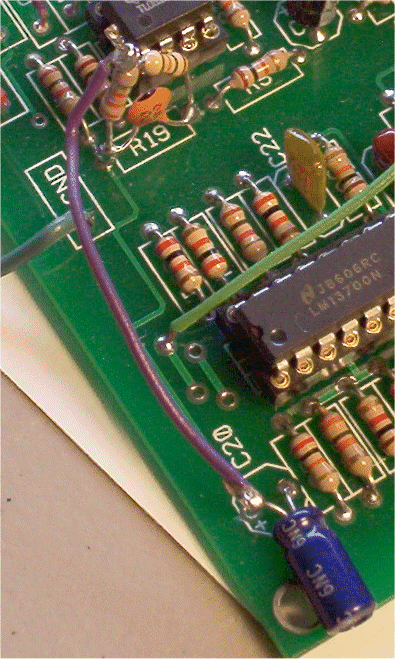
U1-A (and associated components) acts as both the input buffer and the mixer that combines the original signal with the phase shifted sigal via S2 (Four or Eight Stage Selector) and R15 (Feedback adjust pot). U1-B (and associated components) buffers the OUT-4 circuit point which is the output of the fourth phase shift stage. When using 8 stage phasing shifting you get a pseudo-stereo effect by connecting OUT1 and OUT2 to the inputs of a stereo mixing channel. If you change the gain of the input mixer BEWARE of too much feedback from the phase shifted signal. I have found that anything higher than a gain of 1 applied to the fed-back signal and you have an excellent candidate for an alarm system siren. So for example if you choose to change the op-amp gain setting resistor (R19) to 50K you should also change both R15 and R9 to 50K. U2-A and U2-B (and associated components) combine to form a simple but effective low frequency oscillator. U2-B is an integrator that ramps up when U2-A (acting as a comparator)'s output is low and ramps down when U2-A's output is high. U2-A's output goes high when the voltage at its non-inverting input goes above the threshold voltage (ground) and overcomes the current flowing through hysteresis resistor R7. At that time the integrator begins to ramp low until the voltage at U2-A's non-inverting input goes below the threshold voltage (ground) and overcomes the current flowing through hysteresis resistor R7. At that point U2-A goes low and the cycle repeats. R16 controls the rate of the integrator by changing the voltage appearing at R17 and thus the current into (and out of) the integrator. R63 keeps the integrator from seeing ground (which would stop the LFO). If your LFO stops at the lowest setting you could increase R63 a bit (try 150 ohms, 200 ohms etc.). R63 is mounted on the panel. When closed, switch S1 (Tri Ramp switch) bypasses the rate set pot with a diode and a 1K resistor so that during the high cycle of U2-A the integrator ramps down very quickly. During the low cycle of U2-A (as the integrator ramps up) the rate control pot is in the circuit since the diode is reversed biased. You will see a rate shift when you switch from one wave to the other. The ramp will always be about twice the rate of the triangle wave since the integrator discharge is almost immediate in ramp mode. U3-A and U3-B are used in the venerable voltage to exponential current generator. External voltage may be applied to control the phase shift of the unit. The LM13700s are all fed bias current via Q2 (2N3906 PNP) and the 20K resistors in series with their bias pin. The 20K resistors at the bias inputs help to equalize the current into the bias inputs so all of the sections track together pretty well. The phase shift sections are all the same as U4-A (and associated components). The transconductance amp in conjunction with C21 acts to shift the phase of the signal applied to the input (junction of R23 and C21). The angle of shift is dependent on the current flowing through U4-A (which is determined by the control current at it's pin 1 bias input). Each section takes as input the output of the previous stage and adds more phase shift. When this phase shifted signal is combined with the original signal in U1-A, cancellation of frequencies that are at (or close to) 180 degrees out of phase takes place and the characteristic phasing sound is heard. The more feedback applied (via R15) the more pronounced the effect. Several very noticable effects can be heard by experimenting with the settings of R10 and R15 interactively. Although I used all .0047uF caps in the phase shift cells you can change this value (I tried from .001uF to .01uF) or even only change some of them to achieve different sounding phaser effects. Experiment have fun! One last word... If you don't want to use all four LM13700s you can just use the first two (U4 and U5) and just take OUT4 back to feedback to the input mixer/buffer. However using all eight gives you more full cycle phase shifts per modulation cycle and is really... well stunning.
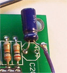
The Stop The Clicks Kludge After putting together the first board I started to play around with it and was enjoying the
great phase effects but I started to hear a ticking. The ticking coincided with the modulation wave form. It was
the fast rise and fall times of the comparator in the triangle/ramp wave generator that was causing it.
In order to slow the rise and fall times that were bleeding
into the signal path and eliminate the ticking
I placed a 20K resistor
between the output of U2-A (pin 1) and the junction of components
R7 (270K resistor), anode of D1 (1N914 diode), and point R16P1.
Additionally a 2.2uF aluminum electrolytic capacitor goes between the
junction of components
R7 (270K resistor), anode of D1 (1N914 diode), point R16P1
and ground. The big yellow block on the schematic shows this.
This kludge is not shown in the PDF schematic (Just so you know).
Also a bit of side info. The ticking sound went away with
a mere .1uF but I decided to go with the 2.2uF because it caused the triangle's peaks to become softer and more
sine like. However the ramp wave does not go fully low with the 2.2uF. You could experiment with the value
for the kludge cap to give yourself the best of both worlds i.e. no ticking and better ramp wave.
You must cut the copper PCB trace that goes from pin 1 of U2A
to the pad for R7. Then place the 20K resistor between
pin 1 of U2-A and the pad for R7. Solder the 2.2uF capacitor's +
lead to the PCB via next to R8 and it's negative lead to C8's ground pad. Here's a picture.
This is really easy and as long as you
hook things up the way the schematic shows you can do it your
way if you like. After cutting the trace you could drill a
couple of holes and mount the comps on the component side of
the board instead of the bottom but that's up to you.
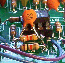
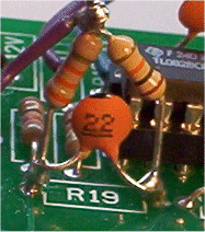
The Increase Output Levels Kludge A diyer who had bought the Phase Shifter board was concerned that the
output levels were too low and that increasing the input level was causing distortion. It is important not to
over-drive the input (or things sound bad) so I had to come up with a fix. I increase the output level and keep the
level the same as it was going into the phase shift array by splitting the feedback resistor around U1-A into
a 10K (R19) and a 33K (R65) and by feeding the phase shifter array from the junction of R19 and R65 where the
level is the same as it was at the output when the feedback resistor was just 10K. Since I went to a gain of 4
in U1-A I added a compensating cap (C30 22pF) to insure that no high frequency oscillation occurs at the output of
U1-A. Op-Amps are usually only compensated internally for a gain of 1. I increased the gain of U1-B by changing
it's feedback resistor to 43K and I also added the 22pF cap for insurance against oscillation. This kludge is
not shown in the PDF schematic (Just so you know).
No trace cutting is required for this kludge just some component sculpture and a short wire. I have included pictures to illustrate
the kludges.
This is also not difficult and as long as you hook things up the way the schematic shows you can do it your
way if you like.
|

| Approx. Current Consumption | |
| +12V | 20mA |
| -12V | 20mA |
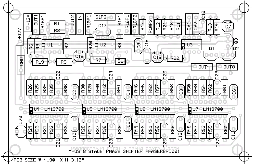
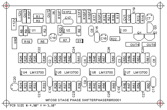
Eight Stage Phase Shifter PCB Parts Layout (Parts Side Shown) PDF
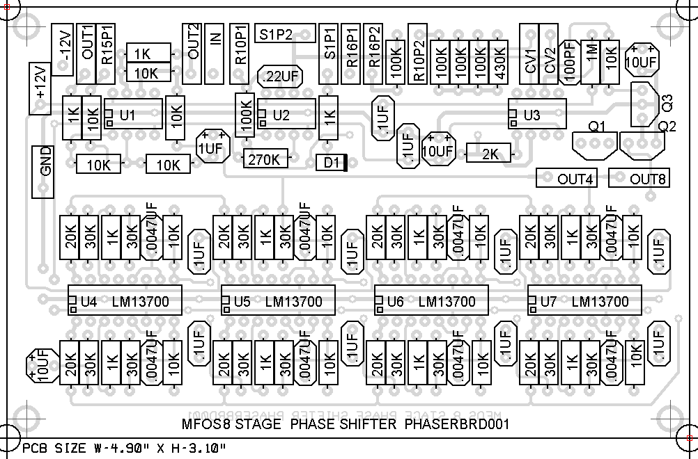
Eight Stage Phase Shifter PCB Part Values Layout (Parts Side Shown)
Eight Stage Phase Shifter PCB Bottom Copper (Parts Side Shown)
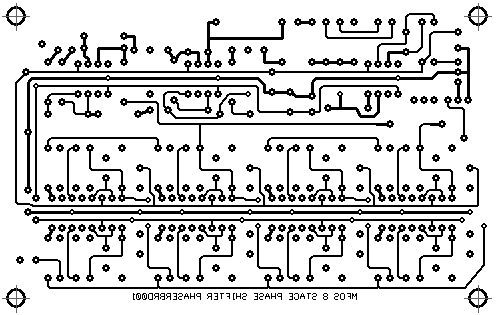
Eight Stage Phase Shifter PCB Top Copper(Parts Side Shown)
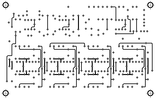
Eight Stage Phase Shifter PCB Top Silk Screen
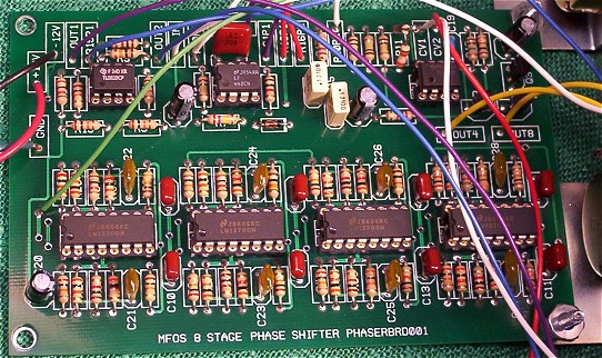
Eight Stage Phase Shifter PCB Populated Larger Image
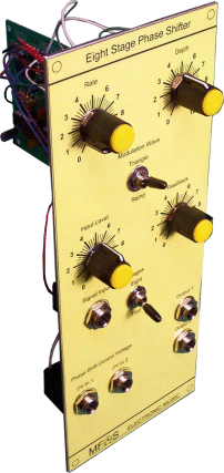
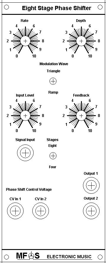
Eight Stage Phase Shifter Front Panel PDF
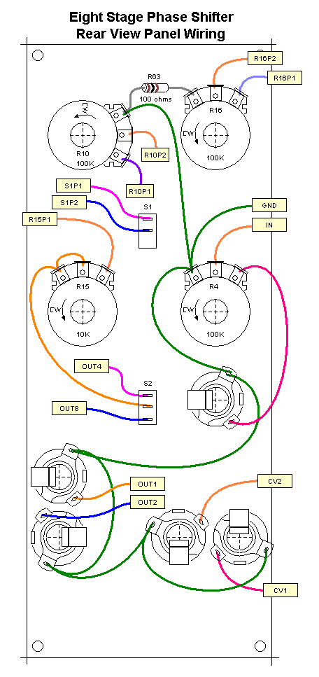
Eight Stage Phase Shifter Panel Wiring Rear View PDF
Eight Stage Phase Shifter Project Parts List
- Using 1% metal film resistors everywhere will reduce temperature related drift.
- Where 1% metal film is specified 5% carbon comp will work but with more temperature drift.
- Usually biFET amps (quads, duals, singles) can be replaced with an equivalent from another manufacturer.
- Capacitors can be film, ceramic, or silver mica.
- LM13700 subs (if applicable) (LM13600, NE5517, AU5517, NTE870).
Eight Stage Phase Shifter Project Parts List
| Qty. | Description | Value | Designators |
|---|---|---|---|
| 4 | LM13700 Dual gm Op Amp(s) | LM13700 | U4, U5, U6, U7 |
| 3 | TL072 Dual Op Amp(s) | TL072 | U1, U2, U3 |
| 1 | 1N914 or 1N4148 Sw. Diode | 1N914 or 1N4148 | D1 |
| 2 | 2N3904(s) | 2N3904 | Q1, Q3 |
| 1 | 2N3906 | 2N3906 | Q2 |
| 1 | Potentiometer | 100K Audio Taper | R4 |
| 2 | Potentiometer(s) | 100K Linear Taper | R16, R10 |
| 1 | Potentiometer | 10K Linear Taper | R15 |
| 5 | Resistor 1/4 Watt 5%(s) | 100K | R18, R21, R20, R12, R17 |
| 14 | Resistor 1/4 Watt 5%(s) | 10K | R14, R5, R2, R3, R9, R33, R36, R39, R41, R61, R60, R58, R55, R19 |
| 11 | Resistor 1/4 Watt 5%(s) | 1K | R31, R34, R37, R40, R51, R52, R53, R54, R8, R6, R1 |
| 1 | Resistor 1/4 Watt 5% | 1M | R13 |
| 9 | Resistor 1/4 Watt 5%(s) | 20K | R24, R26, R28, R30, R44, R46, R48, R50, Kludge R |
| 1 | Resistor 1/4 Watt 5%(s) | 270K | R7 |
| 1 | Resistor 1/4 Watt 5% | 2K | R22 |
| 16 | Resistor 1/4 Watt 5%(s) | 30K | R23, R25, R27, R29, R43, R45, R47, R49, R32, R35, R38, R42, R62, R59, R57, R56 |
| 1 | Resistor 1/4 Watt 5% | 430K | R11 |
| 1 | Resistor 1/4 Watt 5% | 100 ohm | R63 |
| 1 | SPDT Switch | SPDT | S2 |
| 1 | SPST Switch | SPST | S1 |
| 8 | Capacitor Ceramic(s) | .0047uF | C21, C22, C23, C24, C25, C26, C27, C28 |
| 10 | Capacitor Ceramic(s) | .1uF | C2, C4, C3, C6, C8, C10, C9, C13, C11, C15 |
| 1 | Ceramic Capacitor | .22uF | C17 |
| 1 | Ceramic Capacitor | 100pF | C19 |
| 3 | Electrolytic Capacitor (s) | 10uF | C20, C7, C16 |
| 3 | Electrolytic Capacitor (s) | 2.2uF | Kludge C |
| 1 | Electrolytic Capacitor | 1uF | C18 |
Miscellaneous
- 1/16" Thick aluminum plate for mounting the pots and switches.
- Unit is typically mounted in a synth case with other synth modules.
- Assorted hardware 1" 6-32 nuts and bolts, 1/2" #8 wood screws, etc
- Knobs for potentiometers, wire and solder.
- Digital Volt Meter and a Signal Tracer or oscilloscope for testing.