Ray Wilson authored this content while he was actively running MFOS as the founder and resident genius.
We retain the content because it reflects a valuable point of view representing that time and place.
Article by Ray Wilson
Features
- Four separate Three input DC mixers.
- Each Three input DC mixer has normal and inverted output.
- Each Three input DC mixer has output bias control.
- Single sided board layout for easy home production.
Introduction
A DC modulation mixer allows you to combine modulation sources such as an LFO, an envelope generator, and the output of a sequencer and use the combined output to modulate another module. This module gives you a lot of DC mixing flexibility and each of the four three input DC mixers can feed another of the mixers for more flexibility.
Schematics
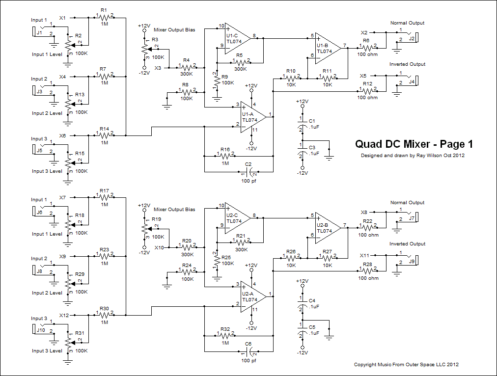
Schematic Page 1
View as PDFThere are four identical three input DC mixers in this module. They can be used separately or the output of one can feed the input of another to expand the number of DC modulation sources which can be addded together. The composite output is then used to modulate a module or modules. I will describe the operation of the first one only as the others operate in the same manner. Only the component designators have been changed to protect the innocent. All ICs are TL074CN quad op amps. They can be replaced with LF444CN for a much lower current module with the same functionality.
Input sources are connected via jacks J1, J3 and J5 which drop the input signal onto potentiometers used as adjustable voltage dividers R2, R13, and R15 (100K level adjust potentiometers). The signal appearing on the wiper of each pot is fed to the input of DC inverting mixing op amp U1-A via mixing resistors R1, R7 and R14 (1M 1/4 watt resistors). The mixed DC signals are fed to the inverting input of U1-A where a gain of one is applied via 1M feedback resistor R16. Capacitor C2 (100pF) suppresses op amp oscillation. The output of U1-A is fed through 100 ohm resistor R12 to jack J5. This is the inverted mixed output voltage.
The output of op amp U1-A is also fed to the inverting input of op amp U1-B via 10K resistor R10 where it is re-inverted with a gain of one (thanks to 10K feedback resistor R11) to reflect the original signal. U1-B's output is fed to jack J2 via 100 ohm resistor R6. The output of U1-B is the non-inverted mixed modulation signal output.
Adjustable bias voltage is applied from the wiper of R3 (whose ends tie to +/-12V) 100K potentiometer via resistive divider R4 (300K 1/4W resistor) and R8 (100K 1/4W resistor) to the non-inverting inputs of U1-A and U1-C. The DC gain of U1-C is adjusted so that both U1-A and U1-B go up and down simultaneously with the adjustment of R3.
If DC signals add up to greater than the supply voltage minus 1.5V they will be clipped. This will not harm the circuit.
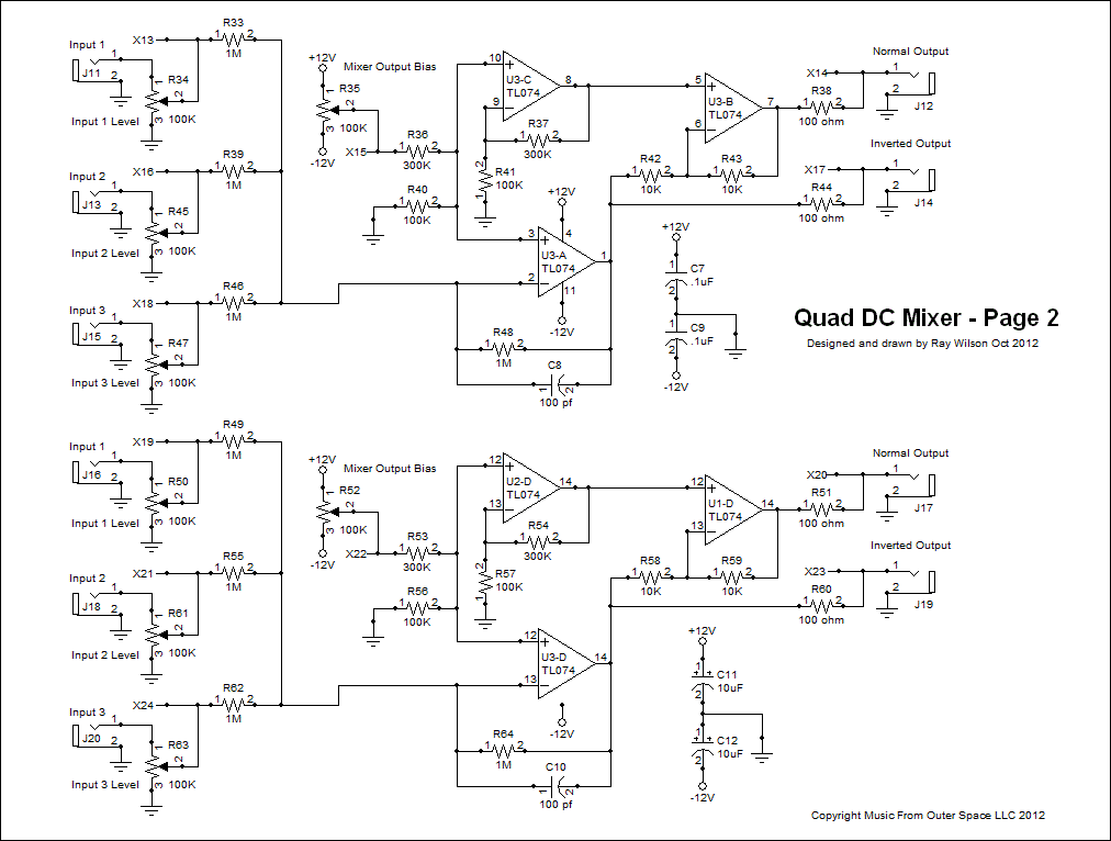
Schematic Page 2
View as PDFSee Schematic Page 1 for Circuit Description
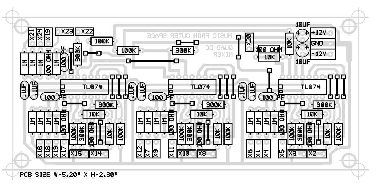
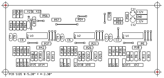
PC Board Information
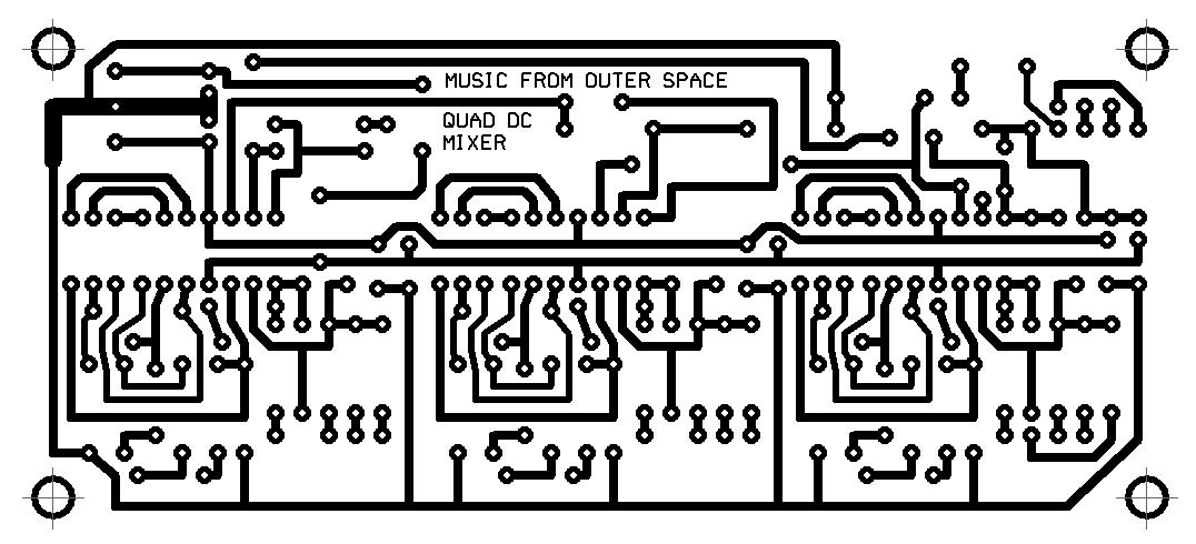
Parts Layout With Component Designators
This is a single sided board that you can make at home. This view shows the designators useful when trouble shooting. All jumper indicators must be shorted with number 22 AWG solid wire or equivalent.

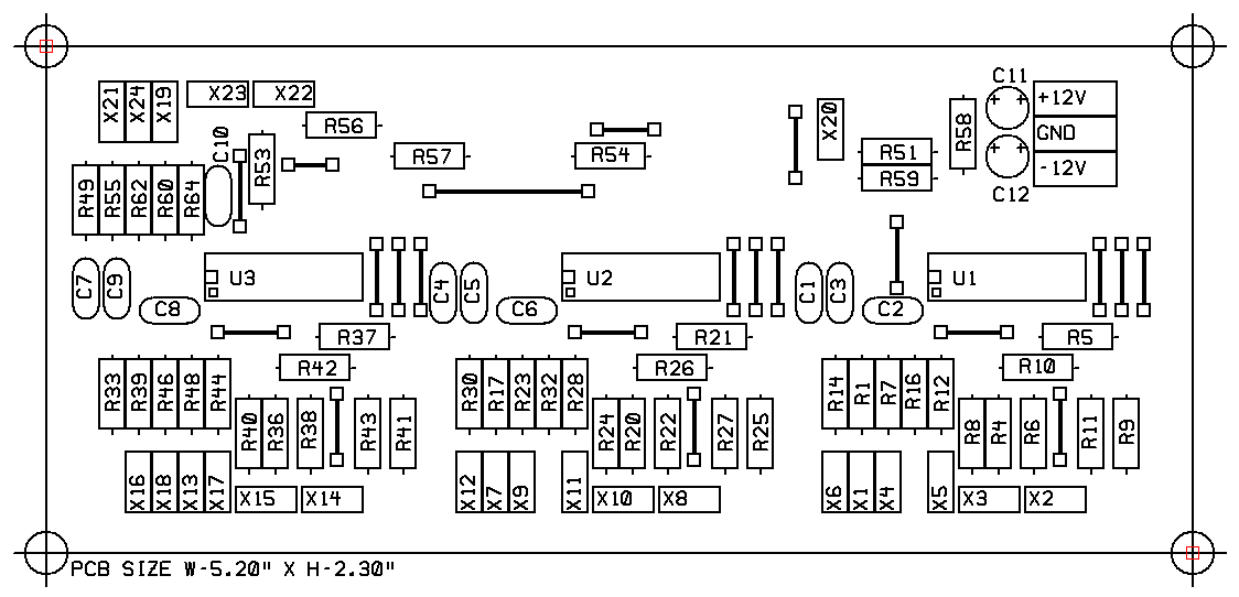
Parts Layout With Component Values
This is a single sided board that you can make at home. This view shows the component values useful when populating the PC board. All jumper indicators must be shorted with number 22 AWG solid wire or equivalent.
Bottom Copper
As viewed from the bottom of the PC board.

Silk Screen
As viewed from the top of the PC board. All jumper indicators must be shorted with number 22 AWG solid wire or equivalent.
Bottom Copper X2
As viewed from the bottom of the PC board.
Silk Screen X2
As viewed from the top of the PC board. All jumper indicators must be shorted with number 22 AWG solid wire or equivalent.
Front Panel Information
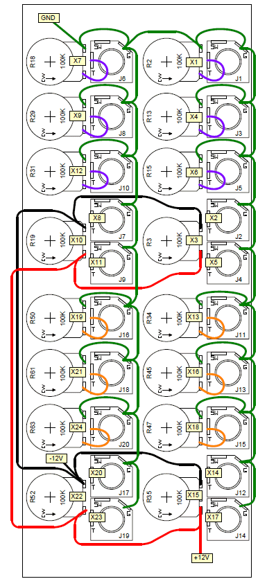
Suggested Front Panel Layout
View as PDFCircuit Description
![]()
Suggested Front Panel Wiring Diagram
View as PDFCircuit Description
Quad DC Modulation Mixer Project Parts List
Component Notes
All cap voltages should be 35V or more. All resistors are 1/4W 5% (1% will work fine). MFOS PC boards use dual inline IC packages. MFOS PC boards usually use 5mm (0.2") cap lead spacing unless it is obvious from the board's legend that it should be larger or smaller. I often specify axial leads for any caps mounted on the front panel but you can use radial as well by adding some wire to the leads.
| Qty. | Description | Value | Designators |
|---|---|---|---|
| 3 | TL074 Quad Op Amp | TL074 | U1, U2, U3 |
| 16 | Linear Potentiometer | 100K | R2, R3, R13, R15, R18, R19, R29, R31, R34, R35, R45, R47, R50, R52, R61, R63 |
| 8 | Resistor 1/4 Watt 5% Carbon Film | 100 ohm | R6, R12, R22, R28, R38, R44, R51, R60 |
| 8 | Resistor 1/4 Watt 5% Carbon Film | 100K | R8, R9, R24, R25, R40, R41, R56, R57 |
| 8 | Resistor 1/4 Watt 5% Carbon Film | 10K | R10, R11, R26, R27, R42, R43, R58, R59 |
| 16 | Resistor 1/4 Watt 5% Carbon Film | 1M | R1, R7, R14, R16, R17, R23, R30, R32, R33, R39, R46, R48, R49, R55, R62, R64 |
| 8 | Resistor 1/4 Watt 5% Carbon Film | 300K | R4, R5, R20, R21, R36, R37, R53, R54 |
| 6 | Capacitor Ceramic | .1uF | C1, C3, C4, C5, C7, C9 |
| 4 | Capacitor Ceramic | 100 pf | C2, C6, C8, C10 |
| 2 | Capacitor Electrolytic | 10uF | C11, C12 |
| 20 | Jack 1/4" 2 Terminal | . | J1, J2, J3, J4, J5, J6, J7, J8, J9, J10, J11, J12, J13, J14, J15, J16, J17, J18, J19, J20 |