Article by Ray Wilson
Some Component Value Changes and Kludges For Improved PerformanceAs I have been experimenting with my Sound Lab I have discovered some mods for improving the operation of the Sound Lab that can be kludged onto the board. If you
are happy with your Sound Lab the way it is... LEAVE WELL ENOUGH ALONE. All of these kludges are optional.
Improving The White Noise GeneratorImproving Oscillator 1 To Oscillator 2 SyncChange R32 to 47KChange VCA Resistor Values For Better Performance |
 |
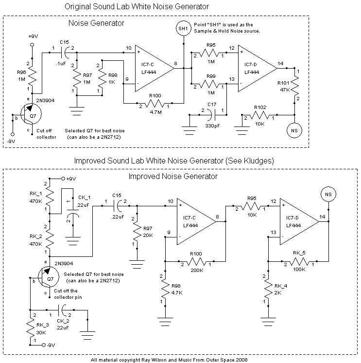
Improving The White Noise Generator
The original sound lab used the noise from the transistor EB junction to create a "digital" noise by feeding it into a comparator and lagging one of the comparator's inputs. The improvement described below creates a higher amplitude white noise and should work with most 2N3904 transistors. It also adds filtering to reduce the feedthrough of power supply noise by adding capacitors at two places in the noise generation circuitry. If you can find some 2N2712 (old school noise transistor) you will probably be able to lower the gain of this circuit. To increase the gain you can make R100 higher in value. To decrease the gain you can make R100 lower in value. Ideally you want about +/- 5 volts (10V P-P) of noise at IC7-D pin 14.Designators with a K (RK_n or CK_n) are Kludge components not originally in the circuit. Please note that components that were in the circuit have changed in value. RK_1 and RK_2 are connected in series and mounted where R96 used to go. A .22uF capacitor (CK_1) goes between the junction of the two resistor leads and ground. This helps filter the supply going to the emitter of Q7. A 30K resistor (RK_3) goes between the base of Q7 and -V. A .22uF capacitor (CK_2) goes between the junction of Q7's base and the lead of RK_3 to ground. This capacitor also filters the supply used to generate the noise on Q7. The impedance to the input of IC7-C has been reduces making it less susceptible to noise. C15 was formerly .1uF and R97 was formerly 1M. C15's value has been increased to .22uF and R97's value has been reduced to 20K. The gain of the first stage of noise amplification has been reduced. IC7-C used to supply a gain of about 4700 (R100 used to be 4.7M and R98 was 1K). Now with R100 at 200K and R98 at 4.7K the gain of the first stage is about 42. IC7-C's output no longer feeds both inputs of IC7-D via 1M resistors. Instead it's output now feeds the non-inverting input of IC7-D via R95 (which has been changed to a 10K resistor). IC7-D is now used for a second inverting gain stage for the white noise adding another factor of about 50. RK_5 is connected between the inverting input of IC7-D (pin 13) and IC7-D's output (pin 14). RK_4 goes between IC7-D's inverting input and ground. Several photos of the required kludge from several angles are shown below to aid you in performing the kludge.
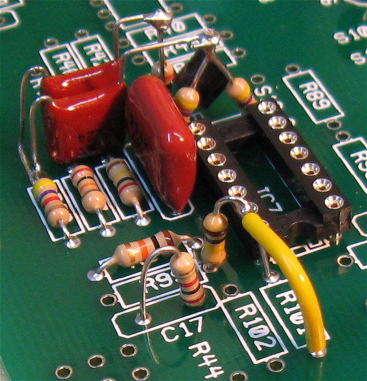 |
Here we see a view of the kludge that shows how IC7-D is made into a gain stage. RK_4 (2K resistor) is mounted where C17 used to go. This
accomplishes connecting IC7-D's inverting input to ground via 2K of resistance.
RK_5 (100K resistor) is mounted using one hole from the former R99 and one hole from the former R101 thus placing it between the inverting input of IC7-D and IC7-D's output. Notice that you must connect a small wire between the lead of RK_5 connected to IC7-D's output and the other side of the former R101. The new values of R100 (200K), R97 (20K), R98 (4.7K) and R95 (10K) are clearly visible in the photo. C17, R99, R102, and R101 are no longer used in the circuit. |
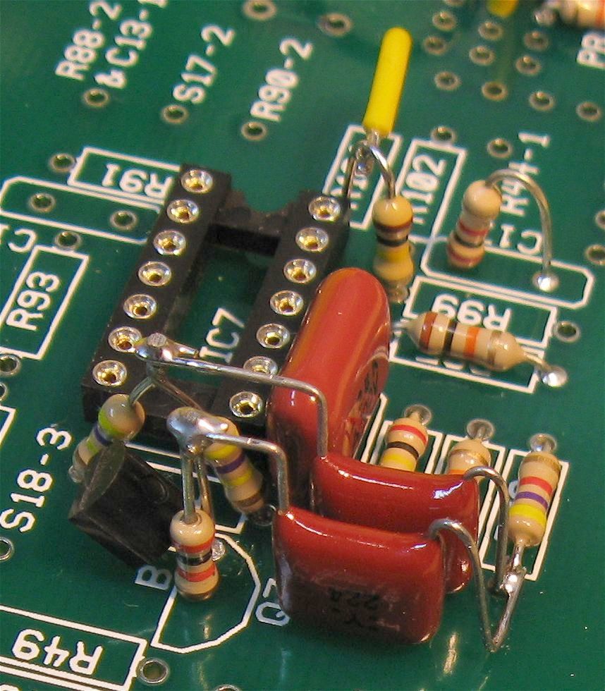 |
Here is the meat of the kludge. RK_1 and RK_2 are connected in series and the two non-connected ends go in the holes of the former R96.
A .22uF capacitor (CK_1) goes between the junction of RK_1 and RK_2 and ground which is the lead of R98 that both CK_1 and CK_2 are soldered to. One end of RK_3 goes into the hole that Q7's base used to go into. The other end of RK_3 gets solderd to the base of Q7 which is bent upward to accomodate the connection. A .22uF capacitor (CK_2) goes between ground (the same ground point used by CK_1) and the junction of Q7's base and RK_3's lead. |
Additional Views For Clarity
 |
 |
Improving Oscillator 1 To Oscillator 2 Sync
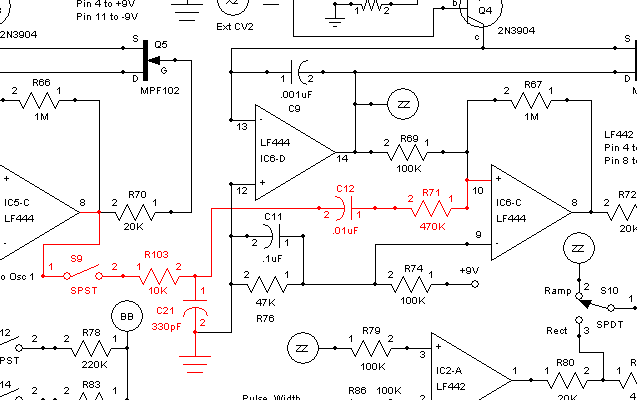
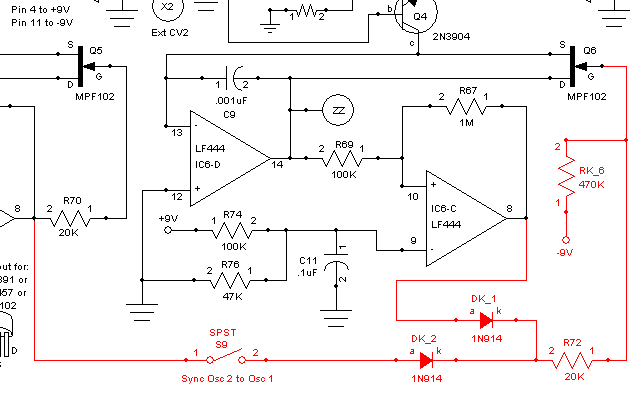
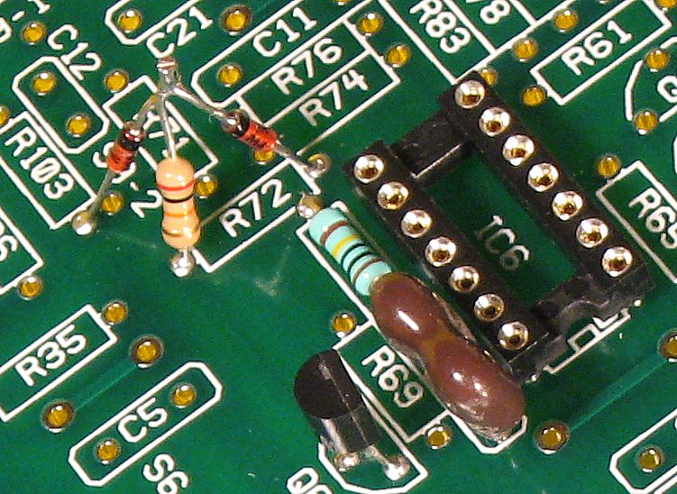
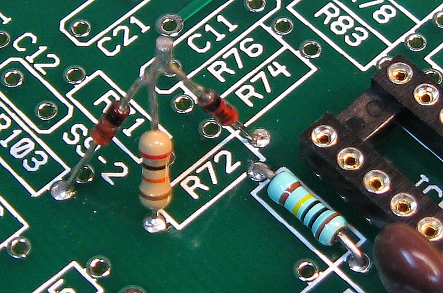
The original Sound Lab's Oscillator 1 to Oscillator 2 sync sent the reset pulse from the output of comparator IC5-C to the non-inverting input of IC6-C via R103, C12, and R71. This would give comparator IC6-C a kick over it's threshold and cause it's output to reset the integrator of Oscillator 2 (IC6-D and C9) via shunting FET Q6. I was not satisfied with the sync generated by this method and I have found a better way which is described below.Designators with a K (DK_n or RK_n) are Kludge components not originally in the circuit. The new method applies the Oscillator 1 integrator reset pulse generated by IC5-C directly to the gate of Oscillator 2's integrator reset FET Q6 via 1N914 diode DK_2 and R72. Previously the output of IC6-C would keep the FET turned off because it's normal state was to sit at -V. Now that current to -V is blocked by the addition of DK_1 (1N914 diode) the gate of Q6 must be held at -V by RK_6 (470K resistor) to -V. In normal mode (S9 open) the positive going pulses from comparator IC6-C go through forward biased diode DK_1 and R72 (20K resistor) to the gate of Q6 causing the integrator of Oscillator 2 to reset. When IC6-C's output is low (approximately -V) DK_1 is reverse biased but RK_6 (470K resistor) holds FET Q6 off.
In "Sync Osc 2 to Osc 1" mode S9 is closed allowing the pulses from Oscillator 1's comparator to reach the gate of Oscillator 2's integrator reset FET Q6. Thus Oscillator 2 is very definitely hard synced to Oscillator 1. In this mode if Oscillator 2 is tuned lower than Oscillator 1, Oscillator 2's integrator never gets a chance to charge completely and thus it's output level will be lower and possibly inaudible (if the frequency difference is great enough). However when Oscillator 2 is tuned higher than Oscillator 1 it will take on a character that sounds almost like filter ringing. This effect is emphasized when the frequency of Oscillator 2 is swept and the range of the sweep is always above Oscillator 1's frequency.
Original Sound Lab Sync Circuit
Improved Sound Lab Sync Circuit
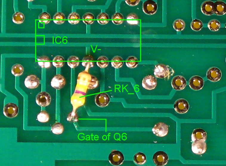 |
On the underside of the circuit board in the vicinity of IC6 carefully solder a 470K resistor (RK_6) between V- (pin 11 terminal of IC6) and the gate of Q6. This resistor will hold the gate low keeping the NFET Q6 off except for when a positive pulse arrives at its gate via R72 and either DK_1 or DK_2. |
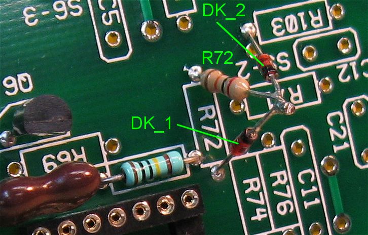 |
Clip the leads of and remove components C21, C12, R103, and R71. Desolder and remove the remaining portions of the leads of these components.
Make a tripod out of DK_1 (1N914), DK_2 (1N914) and R72 (20K resistor) by connecting the cathodes of the two diodes and a leg of the resistor as shown and apply solder to the connected leads. After making the tripod, insert all three components at once and only then solder them in place. Insert the anode lead of DK_1 into the component hole for the side of R72 that connects to pin 8 of IC6. Insert the anode lead of DK_2 into the component hole for the side of R103 that connects circuit point "S9-2". Insert the other lead of R72 into the component hole for the side of R72 that connects to the gate of Q6. |
Additional Views For Clarity
 |
 |
Change R32 to 47K
Not much more to say on this. R32 (formerly 10K) holds the side of the Cut-Off Frequency control to V+. By changing R32 to 47K the filter cutoff frequency control will have a bit more range on the lower end. With 10K it tends to get to the high range too fast in my opinion.
Change VCA Resistor Values For Better Performance
In order to get a bit more amplitude out of the VCA when the AR or LFO control voltages are applied I changed the values of R17 (from 150K to 27K), R18 (from 470K to 150K), R16 (from 470K to 100K) and R20 (from 470K to 100K). Lowering R17 results in a bit less interaction between VCA control voltages. Reducing the values of the other resistors is to compensate for the reduction in R17 and to allow a bit more current to reach the control input of IC3-A. In my Sound Lab this resulted in the ability to get more amplitude out of the VCA.