Ray Wilson authored this content while he was actively running MFOS as the founder and resident genius.
We retain the content because it reflects a valuable point of view representing that time and place.
Article by Ray Wilson
Table of Contents
Sound Lab Mini-Synth PLUS Schematic Page 1

With S2 is in the off state and S3 set to "Trig'd" the circuit functions as follows. When S1 is momentarily pressed it discharges C2 (to about 1.6 volts) through R2 which causes pin 2 of IC1-A to go high. This pushes a positive pulse through C1 and D1 which sets the flip flop made up of IC1-E and IC1-F. IC1-F pin 12 goes high and C3 begins to charge at the rate set by the Attack pot R10 from -8 volts to about 6.5 volts (this voltage is buffered by IC2-B voltage follower) at which point IC1-B's output goes low and IC1-C's output goes high and the IC1-E/IC1-F flip flop is reset by the high logic level presented to pin 13 via D5. This causes IC1-F pin 12 to go low and discharge C3 at a rate determined by R11.
When the "AR Repeat/S&H Trig" switch is in the "AR Repeat" position and the voltage at IC2-B is lower than -6 volts then IC1-D pin 8 goes high and sets the IC1-E/IC1-F flip flop again thus causing the cycle to begin again and subsequently repeat. Notice that I am allowing negative voltages to reach the inputs of the schmidt triggers but that they are protected from drawing high current through their internal protection diodes during that time by the high value resistors in series with their inputs.
When S3 is in the "Gated" position the repeat function is disabled. In this configuration a high level is presented to the "Attack" diode/pot combo as long as S1 is held pressed (because the output of IC1-A is high when S1 is held pressed). Gate mode allows C3 to charge from -8 volts to about +8 volts maximum. When S1 is released a low level is presented to the "Release" diode/pot combo (because the output of IC1-A is low when S1 is not pressed). The output of IC2-B is fed to R15, the AR Envelope output level adjustment pot. The circuit point "AR" is the wiper of R15, which is fed to the AR-Gen switches of the modules.
While contemplating this circuit remember that the inverters are schmidt triggers and that their inputs must go lower than 1/3 of the supply voltage before their output goes high and then the input must go to greater than 2/3 of the supply voltage before the output goes low. This characteristic is know as hysteresis.
The zener on the external gate is meant to protect against gate signals greater than 9 volts. When the gate is high transistor Q8 will discharge C2 the same way switch S1 does.
Resistor R200 has been added and the Repeat switch has been changed to a DPDT (center off) type to allow switching between AR-Repeat mode and AR Gated by the Sample And Hold mode. When the switch is in the center position neither source of AR triggering is used. External triggering or gating can be applied in either mode. For normal manual or external triggering mode the switch should be in the center position.
When the "AR Repeat/S&H Trig" switch is in the "S&H Trig" position the GATE output from the Sample & Hold circuit is fed to the base of Q8 via R200 (100K) current limiting resistor. The end result is that the AR generator is triggered every time the Sample & Hold circuit takes a new sample.
AR Generator Output Level pot R15 is now referenced to ground instead of to -V. This was done to change the range of output from the circuit. Now the output starts at ground and is driven high and low (in relation to ground) as R15 is advanced.
Circuit point "SH1" added to schematic to identify the point used by the Sample & Hold for sampling the AR generator.
The R200 kludge is documented below.
| Connecting the Sample & Hold Gate output to the Sound Lab | |
 |
R200 is mounted as shown. Be sure to mount it on the pads shown because there are kludges to follow
that depend on it being in the right place. Notice it is the last set of connected pads to the
left in the PROTO AREA.
One side of R200 goes to the front panel point marked R200 Pin 2 (which is a pin on switch S2 "Internal Repeat/S&H Trig"). The other side of R200 is connected to a wire which is soldered to the end of 100K resistor R1 that connects to the base of Q8. This mod is used to connect the Sample & Hold gate output to the Sound Lab. |
Sound Lab Mini-Synth PLUS Schematic Page 2
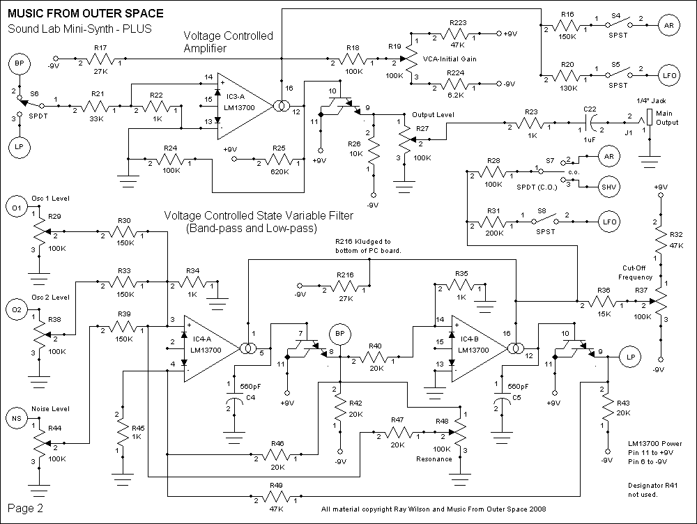
These two circuits are practically straight out of the National Operational Amplifiers Databook data sheet for the LM13700. They have linear voltage control but for a sound box they're fine. The transconductance characteristic of these Op Amps makes them perfect for VCAs and VCFs.
In the VCA the control voltage controls the current flow through the amp and subsequent level of the signal at the output. S4 switches the AR Gen control voltage on or off. When on, the level of the AR Generator output pot determines how much the AR Generator controls the signal amplitude at the output of the VCA. S5 switches the LFO control voltage on or off. When on, the level of the LFO output pot determines how much the LFO controls the signal amplitude at the output of the VCA. R19 controls the initial amplitude at the output of the VCA. When S4 or S5 is on it is best to turn R19 all the way down and then up as needed.
In the VCF the OTAs act as voltage controlled resistors which change the pass-band (in band pass mode) and cut-off frequency (in low pass mode) from low (for low control voltage) to high (for high control voltage). The resonance control adjusts the feedback around the circuit and thus the gain at the cut-off frequency. At high resonance settings the filter rings adding harmonics to the filtered signal which give the classic synthesizer wahhhhh sound when the cut-off frequency is swept from low to high. The filter also acts as the mixer as all of the signal sources are presented to its input via attenuation pots (R29, R38, and R44). It is not necessary to turn the inputs to the filter all the way up. When you do so you can overdrive the filter resulting in distortion (which won't hurt anything and you may even like it). With high resonance keeping the inputs low will keep the filter from peaking into distortion.
The input to the VCA is either the low pass output or the band pass output determined by the setting of switch S6. S7 switches the AR Gen control voltage on or off. When on, the level of the AR Generator output pot determines how much the AR Generator controls the cut-off frequency of the VCF. S8 switches the LFO control voltage on or off. When on, the level of the LFO output pot determines how much the LFO controls the cut-off frequency of the VCF. R37 controls the initial cut-off frequency of the VCF. When S7 or S8 is on it is best to turn R37 off or nearly off.
Several resistor values have changed from the original circuit. This was done to provide more range of control to both the VCF and VCA and to compensate for the fact that both AR Generator Output Level pot R15 and LFO Output Level pot R92 are now referenced to ground.
VCF AR Modulation On/Off Switch S7 was changed from a SPST to a SPDT (center off) configuration in order to allow either the AR generator or the Sample & Hold voltage to modulate the filter's cut off frequency. In the center-off position neither input is connected.
The R216 kludge is documented below.
| Adding R216 To The Bottom Of The PC Board | |
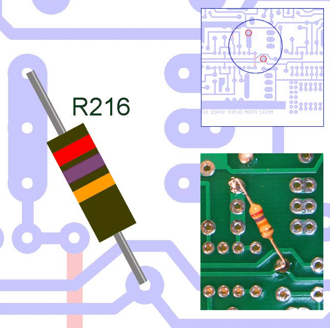 |
R216 is mounted as shown on the bottom of the PC Board in the vicinity of IC4. It goes between -V and a land that is connected to pins 1 and 16 of IC4. |
Sound Lab Mini-Synth PLUS Schematic Page 3

The sound lab uses two voltage controlled ramp oscillators. IC5-B and IC5-A and associated transistors and components comprise a linear voltage to logarithmic current convertor. The control voltages which are summed by IC5-B range from -8 to 8 volts. The corresponding current ranges from around 1uA to 1mA and since the oscillators go up approximately 1 octave every time the current doubles this gives the oscillator a nice range from a sub-audible 0.6 Hz to beyond human hearing.
The explanation of the operation of oscillator 1 follows (oscillator 2 works the same way using its associated components). Oscillation occurs because as the current is sucked out of the input of integrator IC5-D its output goes high until IC5-C (comparator with hysteresis) pin 8 goes high and turns on the N-Channel FET (Q5) which shorts the integrating capacitor (C8) which causes the cycle to begin anew and subsequently repeat. IC6 is used in a similar configuration.
The output of IC6-D (point ZZ) is fed into comparator IC2-A in order to provide a square/pulse wave shaper for Oscillator 2. The control voltage fed into IC2-A pin 2 via resistors R86 and R87 determine the comparator threshold and thus the point at which the output (pin 1) goes high and low. Varying R85 will change the pulse width which will vary the timbre of Oscillator 2 when Rect Wave is selected. S15 permits the LFO output voltage to modulate the pulse width which can cause the output of Oscillator 2 to sound almost like 2 oscillators beating against one another (when approximately 1HZ LFO frequency is used).
S11, S13, S12, and S14 are used to feed the AR Generator, Sample & Hold, and LFO outputs to the CV inputs of the VCOs. When on, you will hear the obvious effect as you advance the LFO and/or Sample & Hold or AR Generator output adjustments.
S9 causes Oscillator 2 to sync to the frequency of Oscillator 1. This provides some very cool timbres which you will hear if you turn on Sync and then tune Oscillator 1 lower than Oscillator 2 and sweep Oscillator 1 upward in frequency.
The fine tuner potentiometers and associated resistors have been added to the schematic since they are an integral part of the Sound Lab Mini-Synth PLUS.
The original Sound Lab's Oscillator 1 to Oscillator 2 sync sent the reset pulse from the output of comparator IC5-C to the non-inverting input of IC6-C via R103, C12, and R71. This would give comparator IC6-C a kick over it's threshold and cause it's output to reset the integrator of Oscillator 2 (IC6-D and C9) via shunting FET Q6. I was not satisfied with the sync generated by this method and I have found a better way which is described below.
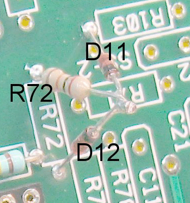
The new method applies the Oscillator 1 integrator reset pulse generated by IC5-C directly to the gate of Oscillator 2's integrator reset FET Q6 via 1N914 diode D11 and R72. Previously the output of IC6-C would keep the FET turned off because it's normal state was to sit at -V. Now that current to -V is blocked by the addition of D12 (1N914 diode) the gate of Q6 must be held at -V by R225 (470K resistor) to -V. In normal mode (S9 open) the positive going pulses from comparator IC6-C go through forward biased diode D12 and R72 (20K resistor) to the gate of Q6 causing the integrator of Oscillator 2 to reset. When IC6-C's output is low (approximately -V) D12 is reverse biased but R225 (470K resistor) holds FET Q6 off.
In "Sync Osc 2 to Osc 1" mode S9 is closed allowing the pulses from Oscillator 1's comparator to reach the gate of Oscillator 2's integrator reset FET Q6. Thus Oscillator 2 is very definitely hard synced to Oscillator 1. In this mode if Oscillator 2 is tuned lower than Oscillator 1, Oscillator 2's integrator never gets a chance to charge completely and thus it's output level will be lower and possibly inaudible (if the frequency difference is great enough). However when Oscillator 2 is tuned higher than Oscillator 1 it will take on a character that sounds almost like filter ringing. This effect is emphasized when the frequency of Oscillator 2 is swept and the range of the sweep is always above Oscillator 1's frequency.
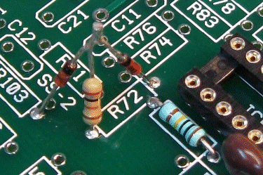
The sync change requires a minor kludge mounted in the area of C12, C21, R71 and R103 on the PC Board. It is documented as clearly as I know how below this section.
The PN4391 NFETs are a good recommendation for replacing the MPF102 NFETs.
| Adding The Fine Tuner Pot Support To The Board | |
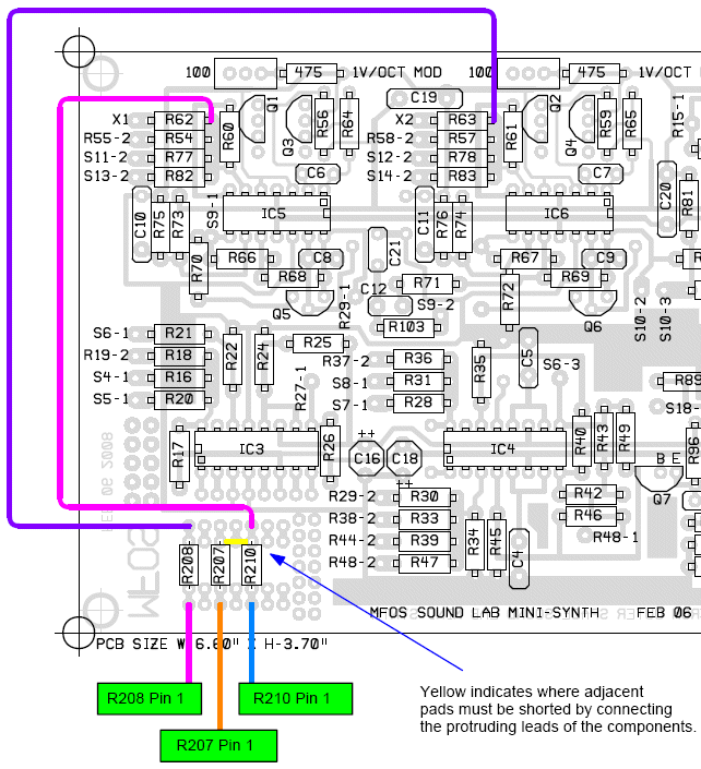 |
R208 is mounted as shown and one side goes to the front panel point named "R208 Pin 1".
The other side of R208 gets attached to a wire that goes to the end of R63 that connects to pin 6 of IC6.
R207 is mounted as shown and one side goes to the front panel point named "R207 Pin 1". The other side of R207 gets attached to it's neighbor R210's lead. R210 is mounted as shown and one side goes to the front panel point named "R210 Pin 1". The other side of R210 gets attached to both the lead of it's neighbor R207 and a wire that goes to the end of R62 that connects to pin 6 of IC5. |
| Adding The Improved Sync Circuitry To The PC Board | |
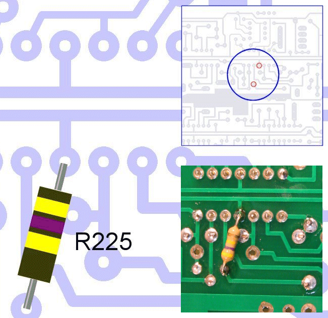 |
R225 is mounted as shown on the bottom of the PC Board in the vicinity of IC6. It goes between -V and a pad that is connected to the gate of Q6. |
 |
If installed, clip the leads of and remove components C21, C12, R103, and R71.
Desolder and remove the remaining portions of the leads of these components.
Make a tripod out of D11 (1N914), D12 (1N914) and R72 (20K resistor) by connecting the cathodes of the two diodes and a leg of the resistor as shown and apply solder to the connected leads. After making the tripod, insert all three components at once and only then solder them in place. Insert the anode lead of D12 into the component hole for the side of R72 that connects to pin 8 of IC6. Insert the anode lead of D11 into the component hole for the side of R103 that connects circuit point "S9-2". Insert the other lead of R72 into the component hole for the side of R72 that connects to the gate of Q6. |
| Additional Views For Clarity | |
 |
 |
Sound Lab Mini-Synth PLUS Schematic Page 4

The modulation selectors and the square wave generation circuitry was moved onto it's own page for clarity. This page is pretty self explanatory and if it's not you may be considering building the wrong project. There are some changes from the original though.
S11 and S12 have been changed from SPST to SPDT (center off) type switches. This is to accomodate the selection of either the AR Generator or the Sample & Hold to modulate the oscillators.
The value of R84 was changed to 220K to change the range of the pulsewidth control slightly.
Inverting Level Shifters (IC8-A and IC8-B) have been added in order to change the ramp oscillator outputs to sawtooth and to bias them to oscillate about ground. In the original the ramp oscillators were taken directly from the integrators in the VCOs. Those signals go from ground to about 5 volts. By making the ramps bipolar (oscillating about ground) the outputs of both the VCA and the VCF are more balanced.
This change requires a major kludge mounted in the PROTO AREA of the PC Board. It is documented as clearly as I know how below this section.
R209 "VCO-2 Mod VCO-1" 100K pot added which allows modulation of VCO-1 frequency by VCO-2's output. R210 is kludged onto the board as shown on the PCB info page.
Sample & Hold Source switching is new to the Sound Lab Mini-Synth PLUS. The blocks that say "June 2011 Micro S&H PCB Connections" (latest Micro S&H version) or "MFOS Micro Sample & Hold Circuit" (previous Micro S&H version) are references to that PC Board. See the new "Micro Sample n' Hold June 2011" project page for details on the new circuit (and a link to the previous version for reference).
| Adding The Level Shifting Inverters In The PROTO AREA | |
| As you can see here the points on the circuit board which were formerly the
outputs of the ramp oscillators are now fed into the inverting level shifters. The outputs of the
inverting level shifters are fed to the rest of the circuitry just as the old points used to be.
Whereas formerly the S10-2 PCB circuit point connected to the front panel at point "W" now the output of IC8-B connects to the front panel at point "W". Whereas formerly the R29-1 PCB circuit point connected to the front panel at point "E" now the output of IC8-A connects to the front panel at point "E". The schematic describes what you see here so I'm not going to give a blow by blow on this kludge. There are photos that tell the tale as well. |
|
 |
Sound Lab Mini-Synth PLUS Schematic Page 5
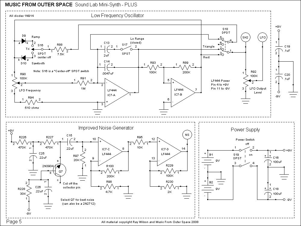
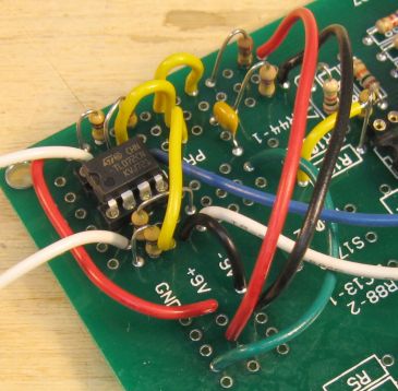
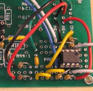
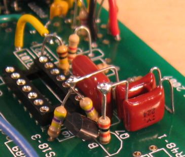
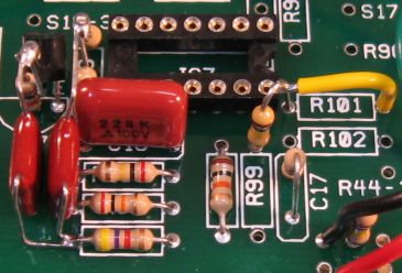
The original sound lab used the noise from the transistor EB junction to create a "digital" noise by feeding it into a comparator and lagging one of the comparator's inputs. The improvement described below creates a higher amplitude white noise and should work with most 2N3904 transistors. It also adds filtering to reduce the feedthrough of power supply noise by adding capacitors at two places in the noise generation circuitry. If you can find some 2N2712 (old school noise transistor) you will probably be able to lower the gain of this circuit. To increase the gain you can make R100 higher in value. To decrease the gain you can make R100 lower in value. Ideally you want about +/- 5 volts (10V P-P) of noise at IC7-D pin 14.
Please note that some components that were formerly in the circuit have changed in value. R226 and R227 are connected in series and mounted where R96 used to go. A .22uF capacitor (C25) goes between the junction of the two resistor leads and ground. This helps filter the supply going to the emitter of Q7. A 30K resistor (R228) goes between the base of Q7 and -V. A .22uF capacitor (C26) goes between the junction of Q7's base and the lead of R228 to ground. This capacitor also filters the supply used to generate the noise on Q7. The impedance to the input of IC7-C has been reduced making it less susceptible to noise. C15 was formerly .1uF and R97 was formerly 1M. C15's value has been increased to .22uF and R97's value has been reduced to 20K. The gain of the first stage of noise amplification has been reduced. IC7-C used to supply a gain of about 4700 (R100 used to be 4.7M and R98 was 1K). Now with R100 at 200K and R98 at 4.7K the gain of the first stage is about 42. IC7-C's output no longer feeds both inputs of IC7-D via 1M resistors. Instead it's output now feeds the non-inverting input of IC7-D via R95 (which has been changed to a 10K resistor). IC7-D is now used for a second inverting gain stage for the white noise adding another factor of about 50. R229 is connected between the inverting input of IC7-D (pin 13) and IC7-D's output (pin 14). R230 goes between IC7-D's inverting input and ground. Several photos of the required kludge from several angles are shown below to aid you in performing it.
The LFO is the same as the Super Simple Ramp and Sawtooth LFO. Notice that the switch is changed to be center off so the circuit produces a triangular wave too. This was suggested by synth-DIYer Harry Bissell (I remembered the little email logo H^) that came with the suggestion.) thanks. Additionally, you can change the range of oscillation for the LFO with the range switch. In low range a 2uF cap (C13) is placed in parallel with the integrator capacitor (C14) to reduce the range of frequency provided by the Frequency pot R90.
Two 9 volt batteries power the circuit and the two by-pass caps absorb the larger current spikes.
Noise circuit change described above. Kludge shown below.
R88 has been changed to 7.5K so that the oscillator maintains more uniformity in amplitude when switching between Ramp, Triangle and Sawtooth.
S18 has been changed from a SPDT to a DPDT in order to insure that when you switch to "Rect" wave oscillation the diodes that cause ramp or sawtooth oscillation are not in the circuit. Formerly if you switched to "Rect" modulation with R16 switched to ramp or sawtooth, the Rect(angle) wave would be so narrow that it was ineffective for modulation. Now when you switch to "Rect" the LFO emits a square wave.
| Improved Noise Generator Kludge |


