Single Bus (1 SPST per key) Keyboard to CV, Gate and Trigger
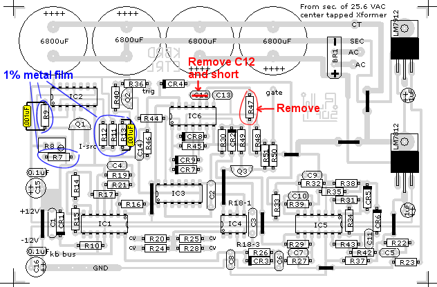
I made some changes that have improved the functionality of this keyboard circuit.- Removed R47. (Superfluous after next step)
- Removed C12 and installed a wire to short pins 9 and 10 of IC6.
- Used 1% metal film for: R7, R9, R11, R12, and R13. (stabilizes current source).
- Soldered a .001uF capacitor across R9 (stabilizes current source).
- Soldered a .001uF capacitor across R13. (stabilizes current source).
- See Schematic Changes and Layout Modifications Below
Please note that the component values shown below can vary by 5% without affecting circuit performance. Some examples: a capacitor value listed as .005uF can be replaced with a .0047uF, a .02uF cap can be sub'd with a .022uF cap with absolutely no problems, 500K can be replaced with 470K.
Cheers and good building!
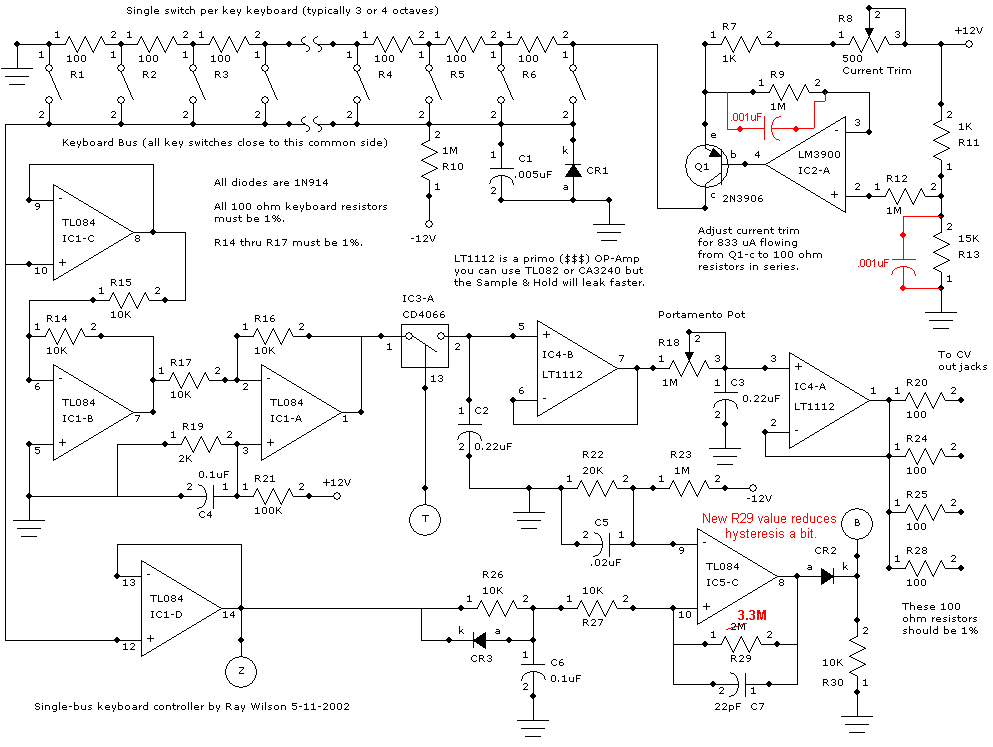
This circuit is designed to produce control voltage, gate and trigger signals for control of an analog
synthesizer which requires 1V/Octave. The circuit requires an electronic organ keyboard with one switch
per key that closes to a common bus (this is a typical electronic keyboard setup). Start by removing any
wires that are connected to the side of the switches opposite the key-bus contact(s). You will need to
solder 1/4 watt 100 ohm 1% resistors between each adjacent key switch (see illustration).

The output of the constant current source which is realized by IC2-A and associated components will be
connected to the high end of the keyboard. The other side will be connected to ground (that is, if you
want notes to get higher as keys to the right are played). The 500 ohm current trimmer is used to adjust
the constant current flowing through the keyboard resistors to be exactly 0.833 mA. This produces a drop
of 83 mV (1/12 of a volt) across each resistor. The keyboard bus is held at a voltage of about - 0.4 to
-0.5 volts by the 1 meg resistor (R10) and diode (CR1) combination.
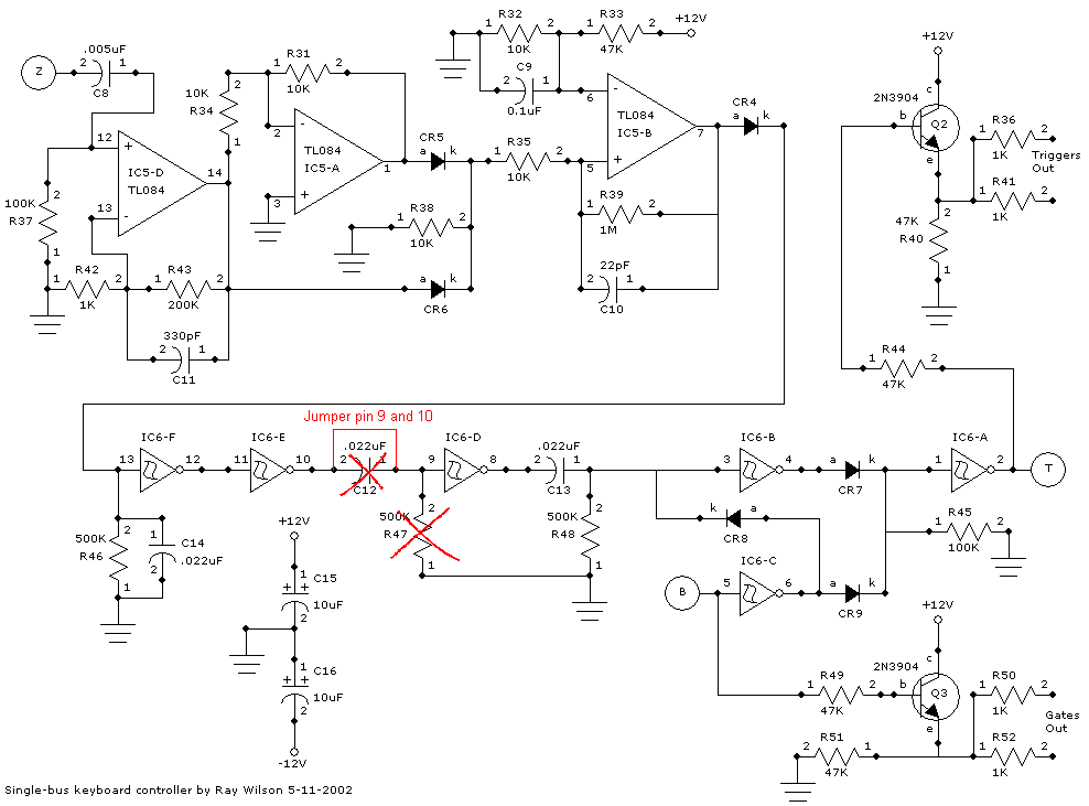
Whenever a key is pressed the keyboard bus assumes a voltage equal to the number of resistors between the pressed key and ground times 83.3 mV. When more than one key is held down the lower note takes precendence. This voltage is buffered by IC1-1C and IC1-D. IC1-D feeds the voltage to a comparator (IC5-C and associated components) and a voltage change detector (IC5-A, B, D and associated components). The comparator produces the gate signal and the change detector produces the trigger and sample and hold pulses.
Some Explanation
You will need a scope to trouble shoot this circuit properly (if you need to). I guarantee you that if you put it together as I have shown, it will work.
When measuring the current output of the constant current source (IC2-A, Q1 and associated components) you need to open the connection between the collector of Q1 and the resistor stack. The current has to flow through your meter in order to be measured so open the connection and put the red lead on the collector side and the black lead on the terminal of the first resistor in the ladder and then you should see 833uA. Start on your meters higher current range so if there is a problem and the current is higher than you expect you don't blow the meter's internal fuse.
With the current adjusted properly you should be seeing voltage on the resistor ladder starting at 0 volts at the ground end and then multiples of 83mV as you go up the ladder toward the current source. So... 83mV on the first resistor beyond ground, 166mV on the next, 249mV on the next, etc. At each octave point you should see a multiple of 1V. If your keyboard starts at C then you should see 0 volts for the lowest key 1V for the first octave, 2V at the next, etc.
You should see a change in voltage every time you press a new key whether you are playing legato or stacato at point Z in the circuit. That point is the raw voltage that appears on the keyboard bus as you press keys. When you are playing legato you get changes of 83 mV per half step. When you play stacato you will get changes from about -0.6 volts to the voltage of whatever key you press.
If all of that is good then your current source is working and R8 is adjusted properly. If you are not seeing the correct voltage intervals then adjust R8 until you do.
IC1 is just buffering the voltage from the buss. As you close keys the bus assumes the voltage associated with the key. When more than one key is pressed it assumes the voltage associated with the lowest note. This is because we are using a constant current source to produce the voltage on the resistor ladder. With no keys down the bus should be at about -.6V due to R10 and CR1.
The outputs of IC1-C and IC1-D should reflect the bus voltage as you press and release keys.
The output of IC1-A will be at about -0.13 volts with no keys pressed or with a key pressed the bus voltage plus 0.4704 volts.
Point Z is connected to IC1-D's output so it will be the same voltage as that. When you press keys you should see the output of IC1-D (which is the raw changing bus voltage) at pin 2 (as you know the caps don't have numbered pins but the schematic numbers them so you know which side I'm talking about) at pin 2 of C8 (the side connected to point Z). The cap will pass the changes in voltage only and not the DC levels so you will see little spikes at the non-inverting input (pin 12) of IC5-D. This is known as differentiation. The spikes will be dropped across R37. IC5-D provides a gain of 200 (actually 201) to the spikes and you should see them as much larger spikes on the output of IC5-D (pin 14). The spikes will be rather dirty because they are generated from the closure of the key switches. But they will go positive when the change in voltage is positive (you went from a lower note to a higher note) or negative if the change in voltage is negative (you went from a higher note to a lower note). The positive going spikes at the output of IC5-D go through CR6 and drop on R38. The negative going spikes are inverted by IC5-A and then go through CR5 and drop on R38. So if you look there you will see a positive spike every time you hit a key no matter which direction you play. Those spike are further amplifed by IC5-B. So you should see -V to +V spikes on the output of IC5-B every time you press a key. The positive going portion of those spikes are dropped on R46. So you should see ground to +V spikes on R46 every time you press a key.
If all of that is good then proceed to the differentiator (IC5-D and associated components). Every time you hit a key or play legato you will see a spike at the output of IC5-D. IC5-D is differentiating the changes in voltage from point Z. The spikes go positive if the change is positive and negative if the change is negative (relative to the last note's voltage). The positive and negative spikes are rectified by IC5-A and associated components (CR5 and CR6). Op amp IC5-B is used as a comparator and you should see a ground to V+ going spike at the kathode of CR4 every time you change notes (-V to +V at the output of IC5-B). If you don't then something is not connected correctly in the differentiator/rectifier/comparator section. The ground to +V spikes out pf CR4 charge C14 and effectively stretch the pulse a bit. The rising edge of the stretched, cleaned-up pulse is dropped across R47 via C12. The pulse is inverted by IC6-D and the rising edge of the inverted pulse is dropped across R48 via C13. IC6-B inverts that pulse which is anded with inverted point B (effectively the keydown logic). The upshot of the whole thing is that the negative going pulse at IC6-B pin 4 is slightly delayed from the edge of the inverted point B signal. This insures that samples (and triggers) are only generated (1) when a key is first pressed (2) when a note is changed with the key down (legato) and (3) NOT when the key is released. The last key down's voltage is the last sampled voltage and not the no-key-down bus voltage (which is about -0.6V). The point T pulses are fed to pin 13 of IC3-A and the current bus voltage is sampled onto C2 which is buffered by ultra-high impedance buffer IC4-B. The output of IC4-B is fed via R18 to the non-inverting input of IC4-A whose output feeds the keyboard's sampled and held control voltage to the world's oscillators, filters and what have you via 100 ohm output protection resistors. (I know the Op Amp outputs are probably short proof but hey why not be belt and suspenders safe).
Timing Diagram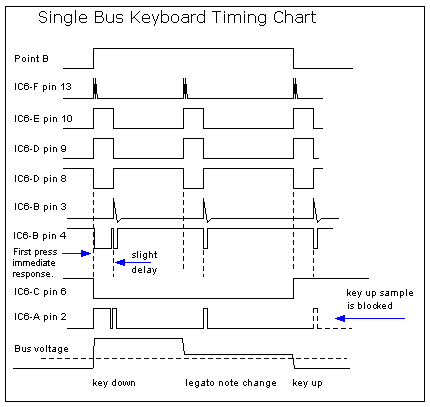
RJW
This circuit works quite well even with my crude setup which involves 3 octaves of piano keys (yes wooden piano keys from an old organ) where each key causes a micro-switch to close when it is depressed. These switches are exceptionally noisy but do not prove a problem for this noise eating design. I mounted the micro-switches on 3 PC boards and connected them to an aluminum rail above the keys. Here are some photos.


I have made a number of improvements to this circuit and solved several problems that plagued the original design.
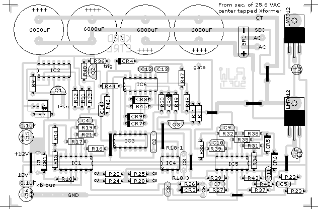
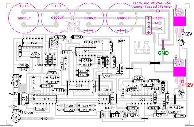
As you can see the PC board includes a + and - 12 volt power supply. If you already have a power supply then don't populate the components for the power supply. BUT... make sure you have power and ground everywhere.
NOTE!! See the PCB layout section below to see which components not to include.
The portamento pot is used to produce a gliding effect between notes as they are played.