Simple MIDI to Control Voltage Convertor
PC-Board and Parts Layout
Disclaimer!
BREADBOARD FIRST... This circuit does not work with all MIDI implementations. test to see if it will work with your synth before you do a lot of work and get disappointed. For a much cooler (albeit more expensive) MIDI to CV circuit go here: PAIA
Introduction
Recently I decided to renew my interest in analog synthesizers. I have designed and built several mono and polyphonic synths in the past and I am planning to make a voltage controlled mono unit so that I can make cool sounds once again with nothing but my own two hands, a century of geniuses inventing affordable electronic components and my trusty Weller soldering iron. If you want to print this article set your printer for landscape so that the images come across all on one page. You can also download the article and then print the images separately.I decided that I was going to crack the MIDI nut so that I could use any MIDI synth's keyboard to play my new analog creation. This MIDI to CV convertor requires no CPU or ROMs to burn and is made from readily obtainable parts. On the other hand it is VERY RUDIMENTARY and provides nothing but control voltage and gate and trigger outputs. If possible turn off everything your synth puts out MIDI-wise except note on and note off. This circuit's performance will depend on your synth's MIDI implementation so breadboard first to see if it works OK with your synth. I am using a Korg X5D for the MIDI source and it rocks.
MIDI to CV Convertor Clock Generation
MIDI Data
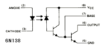
MIDI data is serial in nature and each midi data period is 32 uS long. The MIDI data comes from a MIDI source such as the MIDI out of a synthesizer or computer. MIDI uses a 20mA current loop format to transmit information. The 6N138 opto coupler is used to isolate the sender from the receiver and to translate the current-on current-off information into something we can use (high and low logic levels). Inside the 6N138 is an LED and a photo transistor. The current from the MIDI data is used to turn the LED on and off, the LED's light is used to turn the photo transistor on and off. When the LED is off the photo transistor is off and the logic level at pin 6 of IC6 is high. When the LED is on the photo transistor is on and the logic level at pin 6 of IC6 is low.
Capturing the MIDI Data
The MIDI messages we are interested in are the NOTE ON and NOTE OFF messages since these are the only messages this circuit is designed to respond to. The NOTE ON and NOTE OFF messages are each three bytes long. In MIDI data each byte is preceded by a start bit (always low) and ended with a stop bit (always high). This means that each byte actually requires ten bits to transmit and is 320 uS in length. The three bytes follow each other immediately so the total time for a NOTE ON or NOTE OFF message is 960 uS (see Figure 3 Shift Register Clock Diagram for a picture of what I mean.).The whole purpose of this circuit is to capture the serial MIDI data in shift registers and then convert the note data (which is conveniently binarily coded) from its digital number format to a voltage so that we can control synth modules that require 1 volt per octave (other scalings are entirely possible too with minor tweaks).
Clock Generator
Since MIDI data speed is fixed at 31.25KHz we need to grab the data at the right time so our circuit's timing is critical. We start off with a 2MHz clock module (IC1) and divide this frequency by 8 using IC3 (CD4520 dual binary counter) to arrive at a clock rate of 250 KHz (4 uS period) which is 8 times faster than the MIDI data rate of 31.25 KHz. So now each time MIDI kicks our circuit off we have 8 chances to sample each MIDI data period of 32 uS. The MIDI start bit (high to low) is inverted by IC7 and used to set D Flip Flop IC8 so that IC8's Q1 output goes high and enables counter IC4 to count from zero (where it was patiently waiting) up to 248 at which count it resets both itself and IC8's D Flip Flop #1. The 5 input MML nand gate (formed by R4, associated diodes and 74HC14 invertor) goes low when the counter reaches 248, triggering the MML one shot (formed by R3, C2, associated diode and 74HC14 invertor) to go high and reset the counter and the D Flip Flop in IC8. IC8's Q1 goes low and disables counter IC4's clock input.Now what was that all about you might ask... well I'll tell you. Remember that I said we have eight chances to sample each MIDI data bit. Wouldn't it be great if we could jump up right in the middle of each MIDI data period (which would be 16 uS into the 32 uS MIDI data bit period) and say "Got ya, ya little transient ephemeral logic level". Well we can and thats exactly what we do (plus or minus a piece of one 250 KHz clock cycle or +/- 4 uS).
When counter IC4 counts to 248 we use its Q3 output which goes high right smack in the middle of each MIDI data period to clock 20 of the MIDI data slots into a set of shift registers made up by IC11, IC13 (CD4013 Dual D FF) and IC12, IC14 (CD4094 8-Bit Shift Register/Latch). But didn't I say that the MIDI serial data for NOTE ON and NOTE OFF was 30 MIDI data periods (someone is paying attention)? Yes I did, but we ignore the last set of 10 bits (start-bit, 8-midi bits, stop-bit) because it contains the NOTE ON or NOTE OFF velocity data and all I care about obtaining is the note data which comes in the second byte of serial MIDI data.
When the inverted MIDI data sets IC8's D-Flip Flop #1, its Q output is capacitively coupled to the set input of IC8's D-Flip Flop #2 which is normally held at ground by R6. This causes IC8's Q2 output to go high right along with Q1. We ensure that only twenty clocks of IC4's Q3 get to the shift register clock inputs by decoding IC4's count of 160 with IC9-A and using this to reset IC8's D-Flip Flop #2. IC8's Q2 output allows 20 clocks from IC4 to pass through IC9-B and then it shuts IC9-B off.
Since IC8's Q1 output stays high for 248 x 4 uS or 992 uS it ensures that IC8's D-Flip Flop #2 does not get set again until 32 uS beyond the end of a NOTE ON or NOTE off serial sequence.
Well, now we have the clock pulses at the right times, the conditioned MIDI data, and the STB (strobe) signal which I will explain later. Lets now look at how we get the data into the shift registers.
Figure 2 MIDI to CV Convertor Clock Generation
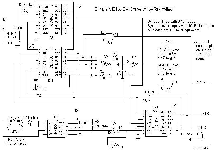
Figure 3 Shift Register Clock Diagram

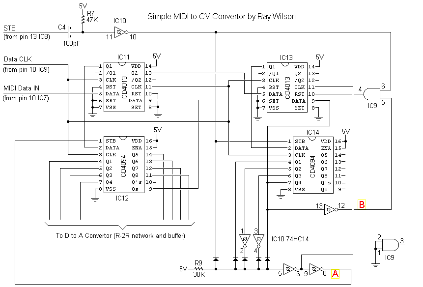
MIDI to CV Convertor Serial to Parallel Conversion
We are going to use IC12 and IC14 (CD4094s) to hold the 8 bit MIDI status data and the 8 bit MIDI note data. We will use IC11 and IC12 (CD4013s) to hold the MIDI stop and start bits. The Data CLK line is connected to all of the clock inputs for IC11 thru IC14 (except for the clock of IC13's D Flip Flop #2).
The Journey Into Parallelism
The MIDI data begins its journey into parallelism at the DATA input of IC11's D Flip Flop #1. It will shift its way out IC11's Q1 into IC12's DATA input, out IC12's Qs output and into the DATA input of IC11's D Flip Flop #2, out IC11's Q2 and into the DATA input of IC13's D Flip Flop #1, out IC13's Q1 and into IC14's DATA in. When twenty clocks (of IC4's Q3) have passed we have captured the status byte and the note data byte in IC14 and IC12 respectively. The observant reader will notice that we let the last stop bit float into oblivion. This bit wasting has a lot of people up in arms but I am able to live with myself.
Just Getting NOTE ON and NOTE OFF
The CD4094 chip is very cool. Not only is it a shift register but it also an 8 bit latch whose inputs are fed by the shift register sections. What this means is that we can shift data through the chip all day and only present data to the outputs when it suits our purpose.In order to ensure that we only get note data associated with NOTE ON and NOTE OFF we pulse the strobe input of IC14 996 uS after the MIDI data starts. Thus the MIDI channel and status data are presented at IC14's Q1 thru Q8 outputs. If the status data indicates that we have recieved a NOTE ON (status 1001) or NOTE OFF (status 1000) MIDI message then we strobe IC12 and permit the note data to appear at IC12's Q1 thru Q8 outputs. Otherwise we do not strobe IC12 and whatever data was present on IC12's Q1 thru Q8 outputs simply remains there.
Figure 4 MIDI to CV Convertor Shift Registers
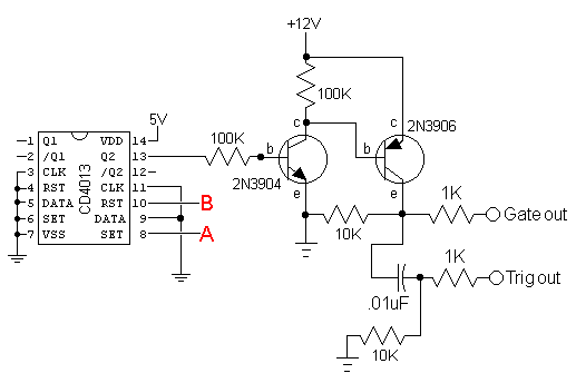
Generating Gate and Trigger (must be built on a small breadboard, not on PC board layout)
The gate and trigger generation circuitry must be placed on a small breadboard and wired into the main board. After a few unsuccessful attempts to generate gate from the MIDI data I finally arrived at this scheme which works with my Korg X5D keyboard. Gate and trigger are generated by using the strobe signal fed to IC12 to set the added flip flop (shown below). The output of pin 12 of IC10 is used to reset the flip flop. This works every time because the strobe always arrives before the rise of pin 12 which happens on key release. The additional components change the output of the gate and trigger to +12V. You need to connect circuit points marked with the red As together and connect the circuit points marked with the red Bs together. The PC layout has these points highlighted.
Figure 4-A MIDI to CV Convertor Gate and Trigger Generator
(must be built on a small breadboard, not on PC board layout).
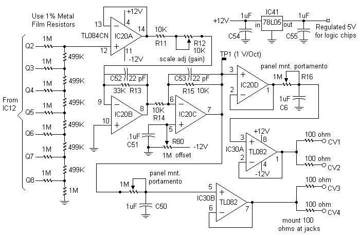
MIDI to CV Convertor Digital to Analog Conversion
The MIDI note data is converted to a voltage using a simple but effective R-2R ladder network and some buffer amplifiers (one trusty TL084 quad JFET op-amp). Although it looks like the Qs are connected to the R-2R backwards they aren't, its just the way the data gets shifted into the CD4094. The V/Oct can be scaled to 1 volt/octave or other scalings by changing the gain of IC20B. To adjust the scale, connect the MIDI up to the circuit and play the lowest note on your keyboard, adjust the offset pot so that you get 0 volts. Now play an octave above that and adjust R12 until you get one volt. You will need to play back and forth with the offset and R12 until you get it right. Once you have it you should get a difference of exactly 1 volt between any two octaves. Both of the portamento pots should be panel mounted as well as the jacks to output the control voltages. Having two portamentos allows you to get some cooler effects than just having one.You can use this D to A convertor from any digital source but remember to connect the data bits opposite of those shown coming from IC12 (i.e. Q8 will be your D0, Q7 - D1, Q6 - D2... etc). The MIDI data gets shifted into the CD4094 backwards so to speak.
The LM78L05 provides the 5 volts needed for the crystal oscillator module and the rest of the digital circuitry. This is the only module in the synthesizer that needs 5 volts so I decided to just put it here instead of in the power supply.
Figure 5 MIDI to CV Convertor D to A Conversion