Ray Wilson authored this content while he was actively running MFOS as the founder and resident genius.
We retain the content because it reflects a valuable point of view representing that time and place.
Article by Ray Wilson
With matched transistors packages becoming scarcer and more expensive it's time to bite the bullet and learn how to make your own matched pairs. The results of hand matching are every bit as good as what you get with the matched pair packages and I'll prove that with examples.
Essentially this article is the combination of Googling for "How to match transistors" and finding help on the web from people like Robert Moog, Bob Pease and articles by staffers at Electronic Design. The consensus is that matching the Vbe of transistors under constant current to within a couple of millivolts is a good way to find transistors that will function well in log convertors and other non-linear circuits. I took what I could find to the workbench and came up with some practical circuits you can use to match transistors. The Moog service manual takes for granted the presence of a +/- 10V supply so I show you how to make a simple one to drive the constant current sources.
The tester is based on the matching technique shown by analog synthesizer pioneer Dr. Robert Moog.
I show three circuits, one to match NPN transistors one at a time, one to match PNP transistors one at a time and one to test two NPNs simultaneously and get a "Go" or "No Go" indication of matching via LEDs. The first two are relatively simple and don't require a lot of highly precise resistors. If you plan to build the third one then you MUST buy 1% metal film resistors in bulk and then measure and select them to obtain .1% precision. If you don't take the time and effort to do that then the circuit will be useless and give you false readings. The circuit measures the difference between two transistor Vbe values and gives you a "Go" light if they are within +/-1.5 millivolts of one another. Actually Robert Moog's advice is that they be within +/-2mV of one another so we are asking a little more than that just to be sure and to make up for a bit of circuit error.
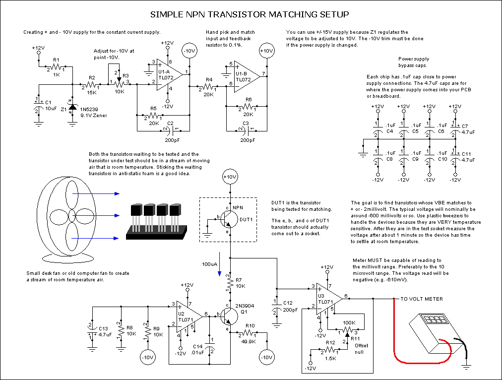
Matching NPN Transistors for Vbe
The top part of the schematic shows the + and - 10V supply that is used to provide voltage to the constant current source. Don't think you can power your next project from this supply because it can only provide a few mA of power but that's plenty for our 100uA (and 200uA for the dual tester) current source.
The voltage provided by the 1N5239B 9.1V zener has a 5% tolerance so it's zener voltage will not be exactly 9.1V but it will be close. We use R3 (cermet multi turn trimmer) to adjust for -10V at the output of U1-A (TL072) pin 1. U1-B (TL072) is an inverting gain of 1 buffer so we get +10V at it's output pin 7. Choose the values for R4 and R6 (20K 1% metal film resistors) so that they match each other within .1%. They don't have to match 20K by .1% just one another. That way the gain of the inverting buffer will be very close to one. The 200 pF caps in the feedback loops of the op amps keep their outputs nice and quiet. There should be bypass caps by each chip's power pins to ground (that is what the cluster of .1uF caps is). There should be 4.7uF electrolytic caps where the power enters the board.
I adapted the Moog service manual's circuit for the constant current sink circuit. Bob Pease also recommends a similar set up in an article he wrote for Electronic Design. I used a TL071 instead of the LM741. Years of op amp improvements have accumulated and the TL071 is miles ahead of the LM741 in just about every important op amp specification. I added a 4.7uF cap (C13) to stabilize the voltage applied to the non-inverting input of U2. I also added a cap in the feedback loop of U2 since it is not being used in the unity gain configuration, again for additional stabilization. R10 sets the current in the sink to 100 uA. Current flows from the +10 volt supply, through the device under test (DUT1) and then through R7 (10K resistor) and into the constant current sink (U2 and Q1 (2N3904 NPN transistor)).
The voltage at the emitter of the NPN device under test will be one Vbe drop below ground. This voltage is buffered by U3 TL071. We have added the offset null adjust pot R11 (cermet multi turn trimmer) to op-amp U3. To null out U3's offset voltage connect it's pin 3 to ground and adjust R11 until you have 0V at pin 6 of U3. The output of U3 is then fed to your volt meter and provides a nice low impedance voltage source. Ideally the volt meter is a 50,000 count meter with excellent precision that can measure parts of a millivolt. Tenths of a millivolt accuracy will work but 1/100s of a millivolt (10 uV) is even better. I use a BK Precision 5491A 50,000 count bench meter. This is a nice meter and I can recommend it.
As shown in the schematic and recommended by non other than Bob Pease (National Semiconductor analog circuit guru) it is a good idea to direct a small fan over the transistors to be tested (which are waiting stuck in conductive foam) and the test circuit so that they are in a stream of room temperature air. This helps the parts to come to a consistent temperature faster and remain there.
Use tweezers to move the transistor under test from the foam to the test socket. I bought some 18 pin ZIF sockets for my test sockets even though I will only be using 3 of the socket pins I figured what the heck it's worth it. For the prototype I built on a radio shack breadboard I used a regular 6 pin machined DIP socket. If you go the ZIF route shop around because I found a variation of about 20 bucks between suppliers. I finally got mine... drum roll... for $3.75 a piece. I bought 10 so now I have a lifetime supply.
After you insert the device to test let a minute of stabilization time go by. After the minute has passed record the voltage and keep track of devices that match (Vbe of both within +/-2mV) however you wish. I like to stick mine in another piece of foam in pairs. Ice cube trays make good storage and you can stick a sticky note with the voltage in the little bin along with the devices. Again the goal is to find pairs whose Vbe match within +/-2 millivolts. I like 2N3904s, they are a nice general purpose NPN and are inexpensive so you can buy a bunch of them to have plenty to choose from. The devices don't HAVE to be 2N3904s and any general purpose NPN will do as long as it has similar characteristics.
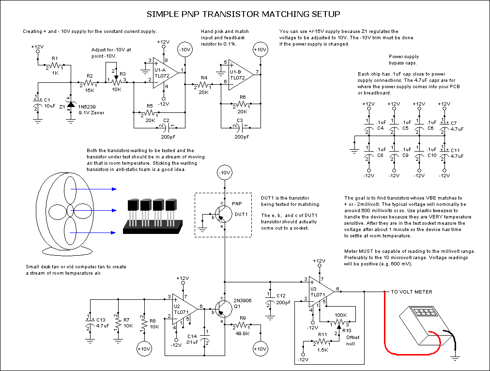
Matching PNP Transistors for Vbe
All of the advice above applies to this circuit except as you can see it is for matching PNP devices. The sense of the constant current has been reversed. Current now flows from the collector of Q1 (2N3906 PNP transistor) into the emitter of DUT1 and drops a Vbe to ground. The voltage at the emitter of PNP DUT1 is positive with respect to ground and will be around 600 mV. Again the goal is to find pairs whose Vbe match within +/-2 millivolts. Note the changes to the biasing network of the constant current generator op amp's non-inverting input.
Matching NPN Transistor Pairs for Vbe With "GO" and "NO GO" Indication.
The goal of this circuit was to give me a go-nogo indication of matching without having to write a bunch of measurements and so forth. It only works if the resistors are hand selected and measured to provide .1% accuracy for just about every part of the circuit. Follow the notes on the schematic if you decide to try and build this. Since we are testing two transistors at the same time I increased the constant current's sink to 200 uA. R18 and R19 serve to balance the current into the sink from the two transistor emitters.
The Vbe voltages of the two transistors are presented to the inputs of two separate unity gain followers (U3 and U4). Both of these op-amps have the null adjust included because it is very important to make sure that each of them have as close to 0V offset as you can get when the non-inverting input of both are grounded.
The outputs of the two unity gain followers are connected to the inputs of a difference amplifier with a gain of 10. Again it is critical that the values of R13 and R16 be within .1% of 10K by selecting them from a batch of 10K 1% metal film resistors. Also it is critical that the values of R15 and R20 be within .1% of 100K by selecting them from a batch of 100K 1% metal film resistors.
This purpose of the difference amplifier is to provide the "difference" between DUT1's Vbe and DUT2's Vbe. So if DUT1 has a Vbe of 612 mV and DUT2 has a Vbe of 620 mV the output of U5 will be (620mV - 612mV) * 10 or 80 mV. The reason we add the gain of ten is so the window comparator made up of dual op amp U6 and associated components which drives our "GO" and "NO GO" LEDs has something it can work with. A comparator needs a couple of millivolts difference between it's inputs before it can decide which way to go, high or low. So if we didn't multiply the difference in Vbe voltages by 10 we would not have enough voltage to make a definite decision.
The window comparator works as follows. R5 (100K 1% metal film resistor), R9 (332 ohms 1% metal film resistor) and R10 (100K 1% metal film resistor) are used to provide the two threshold voltages we need for our window comparator. We use the precision + and - 10V sources and hand pick the values of R5 and R10 to make sure they are within .1% of 100K. This is because we want +15mV for the threshold voltage applied to U6-A's non-inverting input and -15mV for the threshold voltage applied to U6-B's inverting input. When the voltage applied to pins 2 (of U6-A) and pin 5 (of U6-B), the difference voltage, is between -15mV and +15mV the output of both comparators is high and D1 and D2 are reverse biased. Thus +12V through R6 (2K carbon film resistor) is able to both turn on LED1 (the green "GO" indicator) and turn off Q1 (2N3906 PNP transistor) thus keeping LED2 off. If the difference voltage is either below -15mV (minus a mV or two) or above +15mV (plus a mV or two) one of the comparator's outputs will be low sinking the current that was formerly turning on the LED and turning on Q1 which turns on LED2 (the "NO GO" indicator).
Thus if the difference in Vbe voltages between DUT1 and DUT2 is below 2mV we get a green "GO" indicator and if it is above 2mV we get a red "NO GO" indicator. Only by using good construction techniques (keep wires short and place components near the op-amps that use them) and by selecting the resistors as indicated on the schematic to the required precision will this circuit work reliably. I took every precaution when I made my breadboarded prototype and found that I get within 200 uV of the Vbe differences which is good enough with this design to insure that transistors which indicate "GO" are within 2mV of one another.
Calibrating the circuit
With two transistors plugged into the DUT1 and DUT2 sockets apply power and trim R3 so that you get +10.000 volts (+/-5mV) at pin 7 of U1-B. Measure pin 1 of U1-A and insure you have -10.000V (+/-5mV). If you picked R4 and R8 as instructed above for equal value you should see the correct voltages.
Remove the two DUTs and ground the non-inverting inputs of U3 and U4. Measure the voltage at the outputs of each and use the respective null trimmer to adjust both outputs to 0.000 volts +/-.1mV.
Reinsert the two DUTs and short the two emitters together with a test lead. Use the null adjust trimmer of U5 to adjust it's output to 0.000 volts +/-.1mV. Now the unit ready for verification.
Remove the jumper that you used to short the emitters of the DUTs. Allow the devices to be bathed in room temperature air by the fan for about a minute and then measure and record the voltages at the output of U3 and then U4. The output of U5 should reflect 10 times the difference in the voltages you measured. Swap the two DUTs, wait a minute and repeat the measurements. The measurements should be consistent with the former ones and the output of U5 should reflect 10 times the difference in the voltages you measured. This voltage should be very close to the voltage you measured before (but with a different sign) and be within 3 or 4 millivolts of the previous measurement.
Test a number of transistor pairs in this manner. When you get a green "GO" light measure the voltages described above and make sure they are within acceptable parameters. Acceptable parameters are that the voltage at the output of U5 is within about +/- 17 or 18 mV. When you get a red "NO GO" light measure the voltages described above and make sure they are outside of acceptable parameters.
Once you know you can trust the circuit you should calibrate it before each use and then use the lights to indicate "GO" or "NO GO". I plan to build one that takes NPN or PNP pairs and uses a ZIF socket.
![]()
Examples of using the breadboarded version of the "GO" "NOGO" tester.
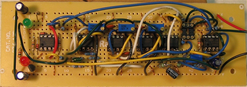
The Breadboard
This is the breadboarded version of the "GO" "NOGO" transistor matcher. You can see the 6 pin DIP socket I am using for this version to hold the DUTs. I plan to build one using a ZIF socket and a switch to go between PNP and NPN matching. The op amp offset null adjust pots and 10V adjust pots are clearly visible. This was a little tight but everything came out fine.
You won't find the 1.5K resistors from the center tap of the null pots to -12V on this board. Some data sheets show them and others don't. I think it's belt and suspenders safe to add them so I put them into the schematics.
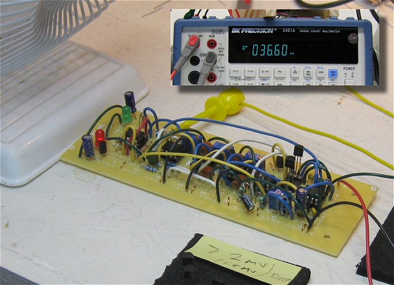
Close But No Cigar...
Here two transistors are under test that do not match. I was still verifying the operation of the breadboard and I have inset the reading on the volt meter. The meter reads about 36 mV which means that the Vbes are about 3.6 mV apart. That's a NO GO!
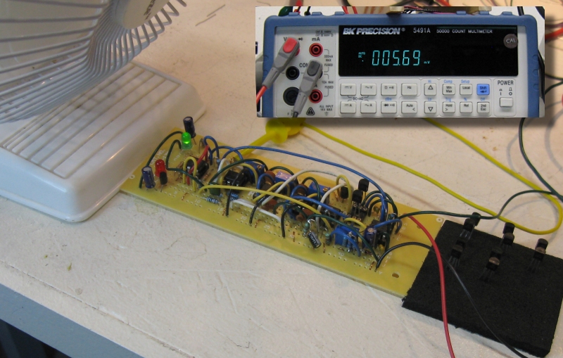
We Have a Winner! (Actually a Nicely Matched Set Of Winners!)
Here two transistors are under test that match quite nicely. I was still verifying the operation of the breadboard and I have inset the reading on the volt meter. The meter reads about 5.7 mV which means that the Vbes are about .57 mV apart. That's a definite GO!
OK I've Got a Matched Pair... Now What?
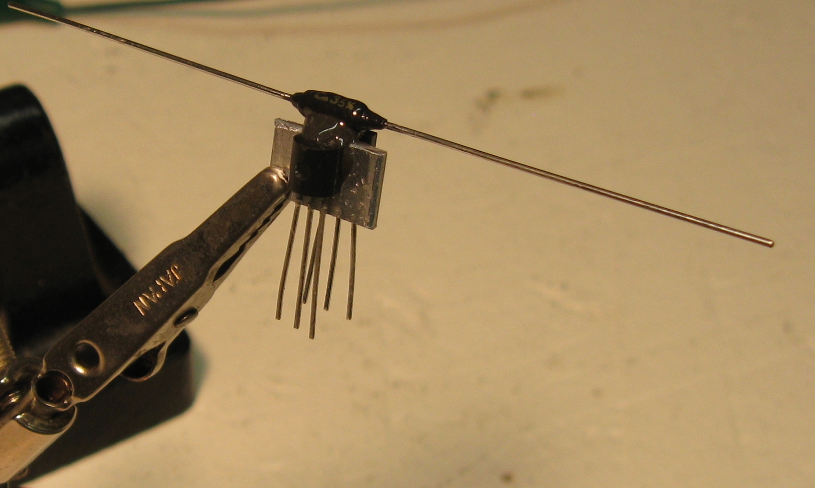
Well now that we have a matched pair we want to do our best to keep them at the same temperature when they are in circuit. To accomplish this Bob Pease suggests that you glue the two transistors to a piece of metal which gives the whole thing more thermal inertia. Going further I glued the temperature compensator to the whole works too. After I install this on the board I'm going to either apply more epoxy to the whole thing being careful not to get epoxy on the leads of anything or make a little cover from some non-conductive material to keep drafts off of the assembly. I used JB Weld two part epoxy (the fast drying kind) and it worked very nicely.
 |
 |
 |
An example of using a hand matched pair with oscillator calibration tips to boot...
MFOS Oscillator Calibration Part I
|
MFOS Oscillator Calibration Part II
|