Range Improvement Modification
(Well... It was kludgeless for a while.)
Article by Ray Wilson
Features
|
|
|
I was bound and determined to get more out of this oscillator design and I really feel like this modification is
very worth doing. However, as I always add, if you like the way your oscillators are working now leave them alone.
I will describe all of the changes and include a bunch of photos of how I did the kludge both for older boards and the latest one.
I modified six of my VCOs with this kludge and I am very happy to say that they all track better and have a greater range than before. These samples are made using three and four oscillators. |
|
MP3 Samples of Extended Range & Better Tracking
Messing about with ramp waves (3 VCOs) Messing about with square waves (3 VCOs) Messing about with the sequencer attached (4 VCOs) Messing about with the sequencer attached (4 VCOs)
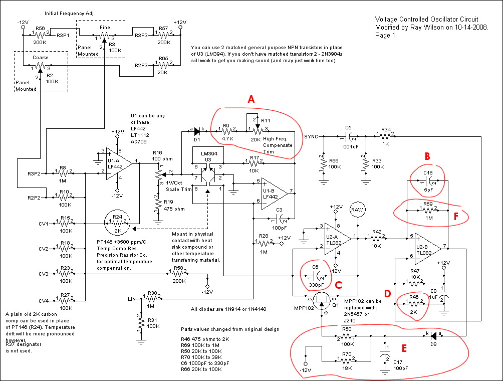
Modified Voltage Controlled Oscillator Page 1 PDF
|
As you can see this is pretty much the same design as the latest oscillator found here. The
changes have been circled and I will go through them one at a time.
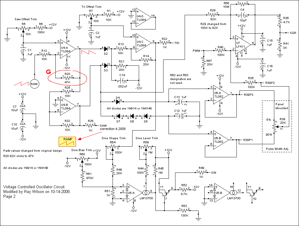
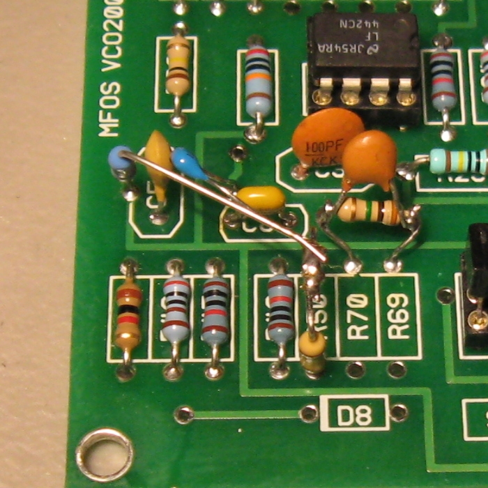
A: The high frequency adjustment in the previous design had very little effect due to the 39K minimum resistance and the 1M trimmer resistor which pretty much nullified the effect as soon as you tweaked it even a little. I experimented with lowering the resistor more and more until I got to 6.2K and I though great I'll just use that. but when I started to see the variation in operation between the 6 oscillators I was trying to get improved performance from I found I had to put a 20K trimmer and a 4.7K minimum resistance to give me the range I needed to compensate for the variation in the 6 test subject oscillators. So change "A" is to replace R9 with a 4.7K 1% metal film resistor and R11 with a cermet 20K trimmer. I used a single turn trimmer and it worked fine but a multi turn will work better due to the increased adjustment precision. (R16 pretty much HAS to be a multi-turn e.g. 10 turns or higher). I'll talk more about this in the calibration section. B: I was resistant to add the positive feedback speed up cap due to it causing the output to saturate and stay high too long but with the change to the N-JFET gate drive for the integrator reset I found that I had to add it to get the output of U2-B to go above ground when it would pulse and turn on Q1. Without it the transistor was not turned on hard enough to reliably short the integrator cap and completely neutralize it. Now the N-JFET turns on nicely and the integrator ramps from the offset voltage of U2-A to about 2 volts and then resets well within 1uS. C: The integrator cap has been changed to 330pF silver mica. The smaller the integrator cap can be and still give clean operation the better. With the relatively low impedance bias network R47 and R46 applying a solid two volts to U2-B's inverting input C6's value was able to be reduced to 330pF from 1000pF. An additional benefit of this is that the cap holds less charge and can be discharged by Q1 faster than a 1000pF cap can. D: R46 changed to 2K so that the bias network of R47 and R46 is a bit higher in impedance to allow the sync pulses to more reliably effect the output of comparator U2-B (and associated components R69 and C18). E: While working on the 10 Step Sequencer I discovered the trick of shoving some charge onto a cap to drive the integrator reset N-JFET gate a little longer. I tried that concept out here and tweaked it until I came up with the values shown. When the integrator ramps slightly beyond the value at the inverting input of U2-B, U2-B's output shoots from -V to +V. Now in the past with nothing but a resistor between the output of U2-B and the gate of Q1 the following would occur. During U2-B's rapid (we're talking sub uSec here) rise from -V to +V, when Q1's gate saw a level of about ground it would immediately (as in nano-seconds) short C6 and cause the output of U2-A to fall below the voltage at the inverting input of U2-B and thus U2-B's output would fall back to -V. Thus U2-B's pulse output would not go far above ground and Q1 while being turned on, was not really being turned on really hard. With the circuit shown the following occurs. When the integrator ramps slightly beyond the value at the inverting input of U2-B, U2-B's output shoots from -V to +V. D8 who was reverse biased now becomes forward biased and allows C17, 100pF cap, to charge. This charge is applied to the gate of Q1 via R50 for a brief period of time. During the time the cap is above ground (sub-uS) Q1 is turned on HARD rapidly and completely discharging C6 (thus resetting the integrator to ground). A parallel path to -V via R70 causes C17 to discharge to -V at which point Q1 is turned off hard. Q1 now has the best of three worlds. It is turned on nice and hard via D8, C17 and R50, turned off nice and hard via R70, and it all happens very quickly. Before I added C18 (positive feedback speed up cap) to cause the output of U2-B to go well above ground I was only able to use the MPF102, J210, and 2N5457 N-JFETs. With the circuit shown you can add the 2N4391 (also PN4391) to the list of useable N-JFETs. F: The positive feedback network around U2-B has been changed from the two 100K resistors and diode to ground to the 1M resistor R69 and the 5pF cap C18 shown in the circuit. This reduces the hysteresis of the comparator and speeds it up a bit. Every little bit of speed improvement in this area of the circuit is important for higher frequency operation. G: With the change in the bias network of R47 and R46 (R46 changed to 2K) the output of the integrator (ramp generator) is now 2 volts. Thus the gain of the wave-shaping circuit had to change to accomodate the new level. Previously R20 (seen on page 2) was 82K giving U4-A a gain of about 8.2. R20 has been reduced to 47K giving a gain of about 4.7. Once you make these changes you will need to tweak the wave-shaping trimmers a bit (see calibraion below). |
Boy are our faces red. The output marked SAW on the PC board is actually... a ramp wave. What was that...? it's a ramp wave. Come again... alright alright I said it's a RAMP WAVE. Somehow in all the confusion the last inversion got missed and we marked it as a Sawtooth. So consider this an embarassing moment and lets all move on.
Modified Voltage Controlled Oscillator Page 2 PDF
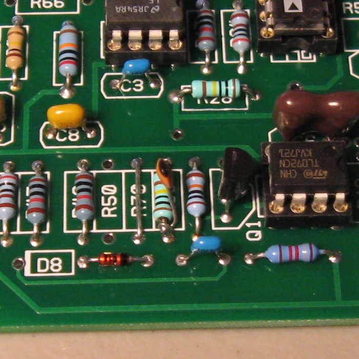
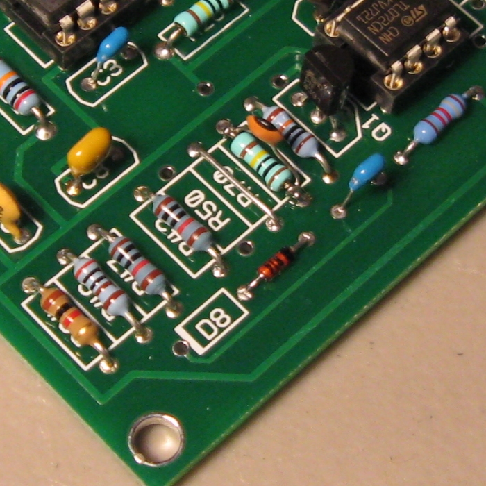
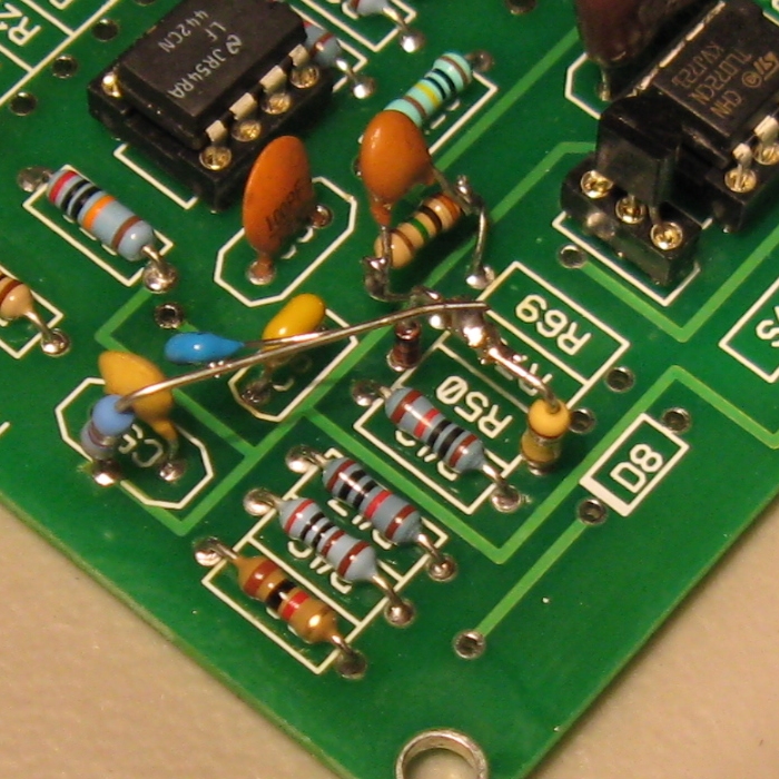
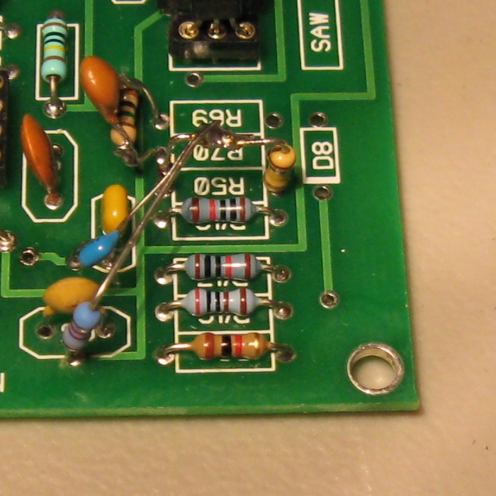
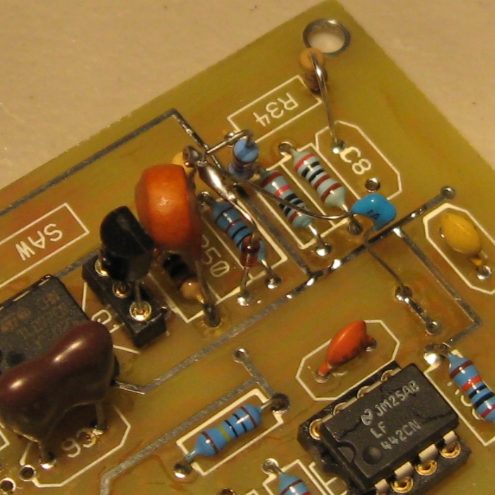
Carefully desolder and remove R69, R70, R50, R9, R20, R11 (trimmer), C6 and D8. I use solder braid and try not to apply too much pressure to lands or donuts. Be careful not to damage
any vias. The designators used in the kludge description reflect the new schematic. Since I was in development of this change to the circuit and
I felt that I was onto a good thing I added pads to the PCB to accomodate all of the necessary changes except the 5pF cap
soldered across R69. See the kludge photos to see where the un-legended components go.
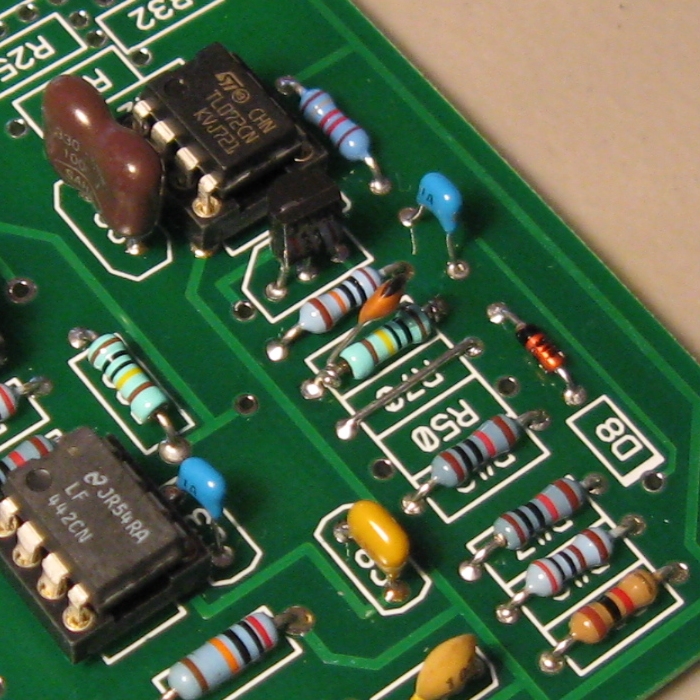
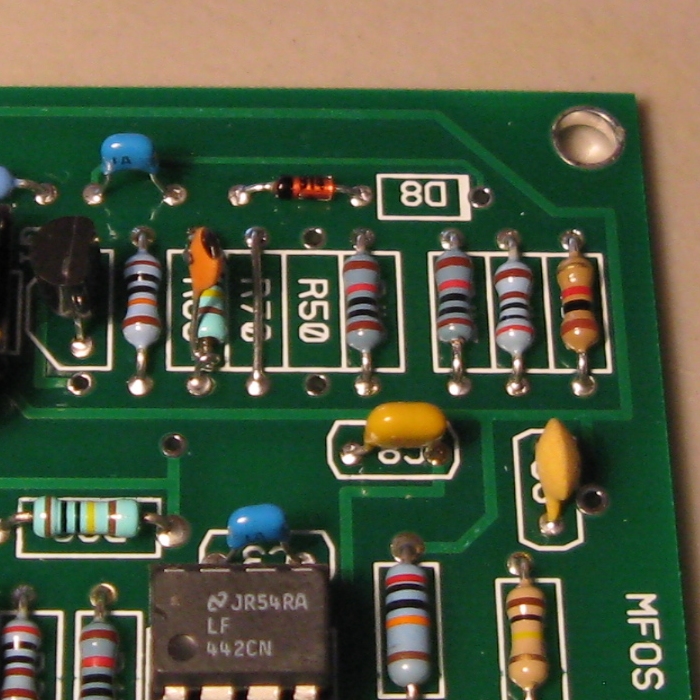
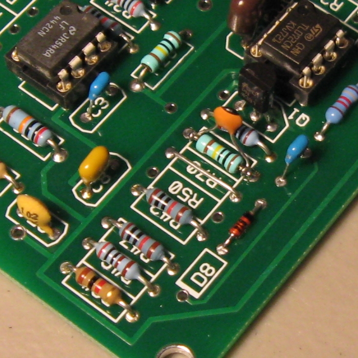
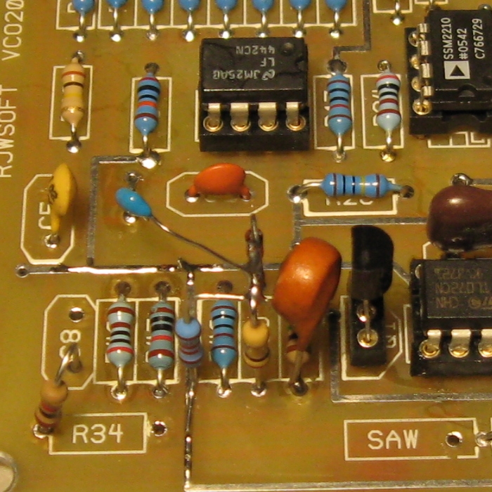
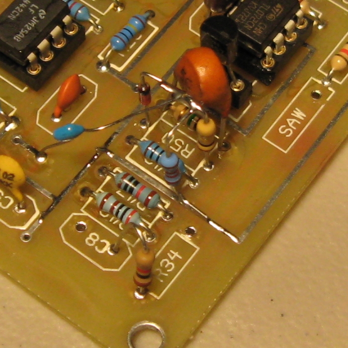
Kludge Photos "REVD Oct 14 2008" Boards (click for a larger view)
 |
 |
 |
 |
 |
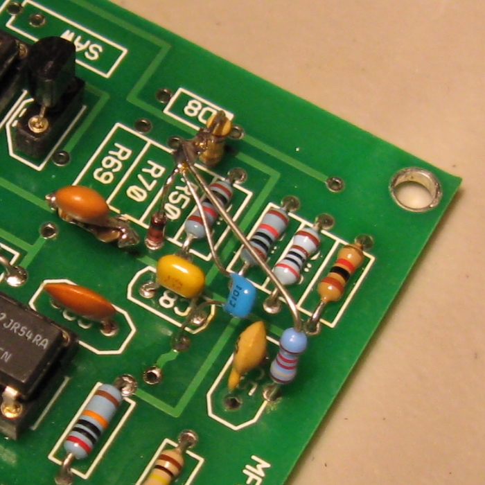
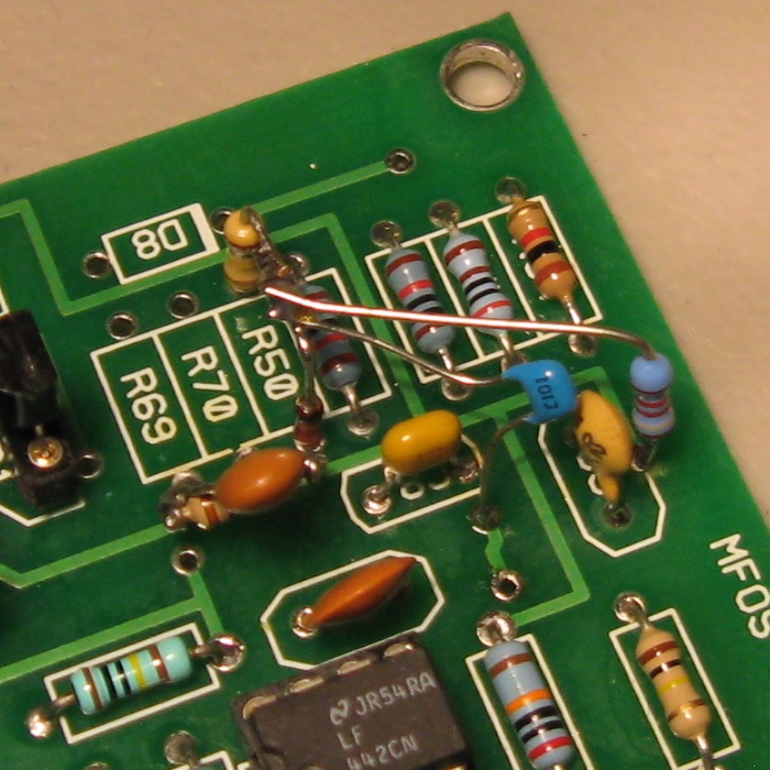
Carefully desolder and remove R69, R70, R50, R9, R20, R11 (trimmer), C6 and D8. I use solder braid and try not to apply too much pressure to lands or donuts. Be careful not to damage
any vias. The designators used in the kludge description reflect the new schematic.
Kludge Photos "Rev 02" Boards (click for a larger view)
 |
 |
 |
 |
 |
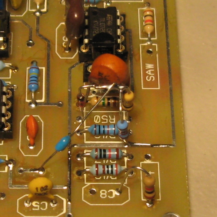
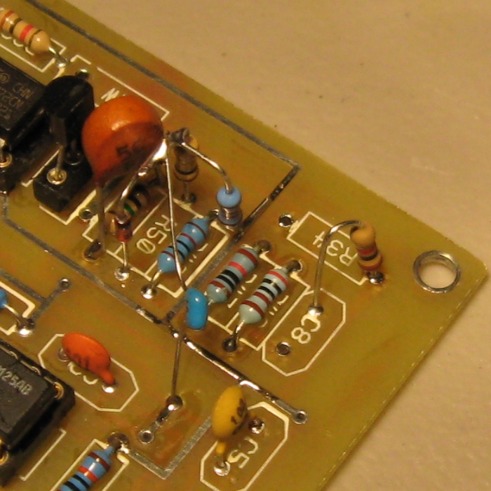
Carefully desolder and remove C8, R37, R50, R9, R20, R11 (trimmer), and C6. I use solder braid and try not to apply too much pressure to lands or donuts. Be careful not to damage
any vias. The designators used in the kludge description reflect the new schematic.
Kludge Photos Older Boards (click for a larger view)
 |
 |
 |
 |
 |
Voltage Controlled Oscillator Calibration (Somewhat tedious to be sure)
|
Before you do the scale adjustments go through the waveform processing adjustments explained on this page.
The change in R20's value will cause a need for readjustment of the saw, triangle and sine offsets (do them in that order).
You will need a good voltage source that is accurate to a least a millivolt or so that can be adjusted from 0 to 10V. A 1V/Oct synth keyboard is a perfect choice. You will need an accurate volt meter. You will need a frequency counter (or a really good ear). Connect the adjustable voltage source to one of the CV inputs (other than the linear one) and set it's output to 0V. Connect the frequency counter to one of the outputs. Listen to another one through an amp (I prefer the sine).
|
VCO Modification Parts List
| Qty. | Description | Value | Designators |
|---|---|---|---|
| 1 | 4.7K resistor 1% metal film resistor | 4.7K | R9 |
| 1 | 100K 1% metal film resistor | 100K | R50 |
| 1 | 18K 1% metal film resistor | 18K | R70 |
| 1 | 47K 5% carbon resistor | 47K | R20 |
| 1 | 20K Cermet Trimmer Pot | 20K | R11 |
| 1 | 2K 1% metal film resistor | 2K | R46 |
| 1 | 1N914 Diode | 1N914 | D8 |
| 1 | 330pF silver mica cap | 330pF | C6 |
| 1 | 5pF ceramic cap | 5pF | C18 |
| 1 | 100pF ceramic cap | 100pF | C17 |