Ray Wilson authored this content while he was actively running MFOS as the founder and resident genius.
We retain the content because it reflects a valuable point of view representing that time and place.
Article by Ray Wilson
Features
Possible Quirks
Audio SamplesAdjusting sequencer knob (Half Steps) Adjusting sequencer knob (Whole Steps) Adjusting sequencer knob (Fourth Steps) Running sequencer (half, whole, fourths) Ramp wave (half, whole, fourths) Sample and Hold (half steps) Slow Sample and Hold (half steps) w/glide Sample and Hold (whole steps) Sample and Hold (fourth steps) |

My twins (two dual quantizer modules). |
Minor Performance Improvement (Integrated into documentation)
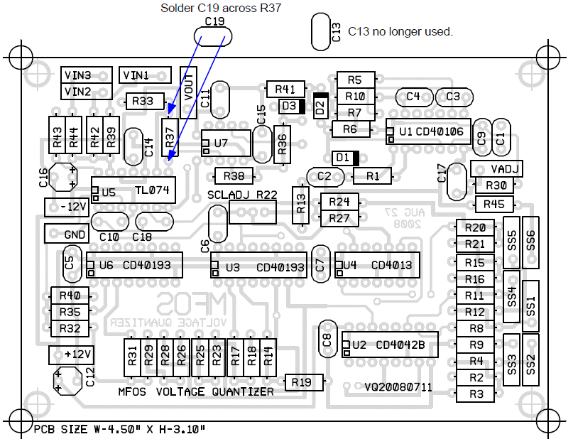
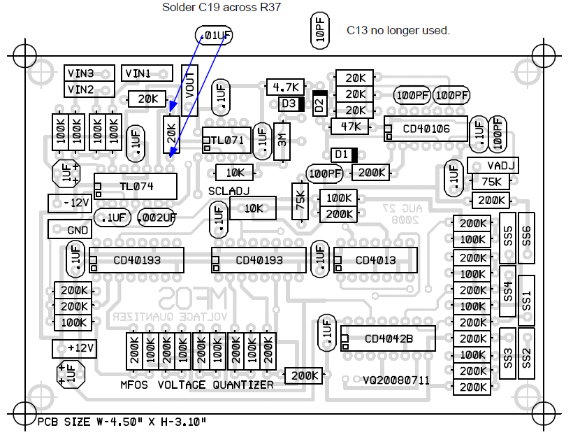
I have eliminated comparator speed-up cap C13 (10pF ceramic cap). I found that without the cap their is less chance for output jitter. This change makes the A to D convertor used in the front end of the quantizer more stable.
I have increased the value of output voltage glitch supressor C18 to .002uF. This results in less digital noise on the output of the quantizer.
I soldered a .01uF cap across the feedback resistor R37. This reduces the digital noise appearing on the output of U5-C and reduces jitter since the comparator is presented with a cleaner voltage.
R1 must be a 200K resistor. Make sure the clock frequency is between 40KHZ and 50KHZ. Clock rates above 50KHZ will increase jitter.
Lastly for greatest accuracy. I ordered 100 each of the 100K and 200K metal film resistors and then used an accurate bench meter to further sort them to find resistors that were within 0.1% of 100K and 200K respectively and then used those in the A to D and D to A R-2R circuit sections. By doing so I got excellent accuracy in the output voltage.
With these changes I am very pleased with the operation of this circuit. All four are operating quite nicely.
Introduction
A voltage quantizer takes a continuously variable input voltage and outputs a stepped (or quantized) voltage. Whereas the input voltage might ramp up from 0 to 1V continuously the output voltage of the quantizer will be discrete steps of .083V. In normal mode this quantizer always starts at digital 1 or .083V. As the input voltage starts to ramp from 0 up to 1 volt the output will step to .1666V, .2499, .3332, etc up to 1.0V. The circuit also features a whole step mode in which the in to out conversion is quantizd to steps of .1666V. It also features a fourth step mode in which the in to out conversion is quantizd to steps of .3332V. Useful with sample and hold circuits to bring voltages into musical scale steps (half, whole or fourths). Useful with sequencers to bring voltages into musical scale steps (half, whole or fourths).
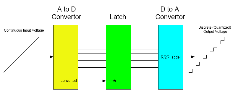
MFOS Voltage Quantizer Block Diagram
|
The MFOS Voltage Quantizer uses an A to D followed by a D to A to produce the conversion from continuous input voltage to quantized (or discretely stepped) output voltage. There are several ways to implement an A to D convertor. The MFOS Voltage Quantizer uses the method in which a voltage is compared with a digitally generated ramp voltage (using the R/2R technique). When the digitally generated ramp voltage goes above the level of the input voltage the count used to generate the voltage is stored in a latch. The output converts the latched count using a R/2R D to A to produce the discrete output voltages.
|
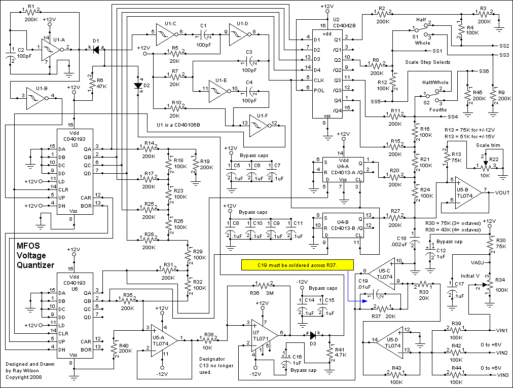
MFOS Voltage Quantizer Updated Schematic Page 1 PDF
|
U1A (inverting schmidt trigger) is connected as a square wave generator (with R1 and C2) and is used as the main clock for the circuit. Frequency is approximately 50KHZ. The spec sheet for the CD40106 shows that there is variability in the astable operation related to the device's threshold levels. Since that is the case, it is a good idea to measure this frequency and if it is too high or low adjust the value of R1 to compensate. Making R1 higher in value will reduce the frequency and making R1 lower in value will increase the frequency. There is nothing magical about the frequency being exactly 50KHZ. However going higher in frequency will increase the possibility of jitter. I would recommend the frequency be between 40KHZ and 50KHZ and the value for R1 to be between 200K and 240K. Being within 10KHZ on the low side will work fine. U1-A's output is inverted and used to clock the 8 bit counter (made up of two CD40193 Synchronous 4-Bit Up/Down Decade Counters). These counters were selected because they are synchronous and thus have a minimal amount of inter-count overlap between the outputs which results in unwanted glitching at the converted voltage output (explained later). U1-B's output is connected to the UP clock input of U3. U3's CAR (carry) output is used to clock U6 and thus the counters are cascaded and act as one 8 bit counter. Only the first 6 of the outputs are used for the A to D convertor. U3's BOR (borrow) output is connected to U6's DN (down) count input. The counters never reverse direction so this function is never actually used. The DN (down clock) input needs to be terminated and this accomplishes that. The jam inputs are all grounded because the pre-load function is not used. The LD (load) inputs are connected to +12V to stabilize them. Why didn't I just use the CD4024 (seven stage ripple counter)? I experimented with the CD4024 (seven stage counter) but abandoned it due to the fact that ripple counters exhibit more inter-count overlap in their outputs. The CLR (clear count) inputs are wired together and are used to zero the counters after a voltage is sampled. Thus the conversion happens faster for lower voltages (since less counts occur between resets) and takes a bit longer for higher voltages (since more counts occur between zeros). The conversion happens faster than most people's ears can detect and is thus quite adequate (usually .5 to 1.5 milliseconds). The outputs of the counter made up of U3 and U6 feed an R/2R ladder which converts the counter's output to a voltage that is proportionate to the count. Thus as the counter's output counts from 0 through to 63 the voltage appearing at the non-inverting input of U5-A proceeds from 0 to about 7 volts. It does so in discrete steps of (7/63 V or about .111V). So for example, 0 = 0V, 1 = .111V, 2 = .222V, 3 = .333V, ... to 63 = 7V. Let's say that the "Initial V" control is adjusted so that 1 volt appears on the output of U5-C and no other voltages are being fed into any of the inputs. This will result in 1 volt sitting on the the inverting input of U7 which is used as a comparator. Normally the output of U7 is low (-12V). When the count steps to a level that causes the voltage on U7 pin 3 (non-inverting input) to go above the voltage on U7 pin 2 (inverting input) the output of U7 shoots from -12V to +12V. This causes the voltage on R41 to go from ground to approximately +11.5V. Diodes D1 and D2 in conjunction with R6 and U1-C form a NAND gate. When U1-A's output is low diode D1 conducts and the voltage at the junction of D1, R6 (47K) and D2 falls to about .6V and thus U1-C's output is forced high. Additionally, when U7's output is low (-12V), D3 blocks current in the reverse direction, D2 conducts via R41 (4.7K) and brings the junction of D1, R6 (47K) and D2 to about 2 volts and again U1-C's output is forced high. Only when the output of U7 (pin 6) and the output of the clock generator U1-A (pin 2) are simultaneously high will the output of U1-C (pin 6) fall low because only then is nothing pulling the voltage at the junction of D1, R6 (47K) and D2 low which allows +12V through R6 to hold U1-C's input high. Now it is important to note that the counter advances on the positive going edge of the output of U1-B. And U1-B's output is inverted from U1-A's output. When the counter steps up to the count that causes the voltage on U7's non-inverting input (pin 3) to exceed the voltage on it's inverting input (pin 2) U1-A doesn't go high until a half clock period later. This delay helps to reduce the effect of inter-count glitches that might corrupt the linearity of the A to D. It allows a half clock period before sampling whether the output of U7 is solidly low or high. Subsequently, if U7 is high when U1-A's output goes high U1-C's output falls low and the following occurs. The low going edge of U1-C's output pulls U1-D's input momentarily low via C1 resulting in a very narrow low to high pulse at the output of U1-D. This pulse is used to latch the low six bits of the 8 bit counter formed by cascaded counters U3 and U6 into the six bit parallel latch formed by CD4042 (Quad Clocked D Latch) and the CD4013 (Dual D Flip Flop). The falling edge of the narrow pulse at the output of U1-D pulls the input of U1-E momentarily low via C3 resulting in a very narrow low to high pulse (2uS) at the output of U1-E. The falling edge of the narrow pulse at the output of U1-E pulls the input of U1-F momentarily low via C4 resulting in a very narrow low to high pulse (2uS) at the output of U1-F. The pulse at the output of U1-F is used to reset the counters to 0. Essentially this cascade of narrow pulses causes a slight delay (2uS) between the latching of the count and the zeroing of the counters. Thus our sampling of the input voltage, latching, and counter clearing are all done synchronous to the main clock. Calibration The latched count is fed to another R/2R ladder which comprises the output of the Voltage Quantizer. The output R/2R output is scaled via trimmer R22 (Scale Trim) to provide .0833V per step conversion. To trim the pot set S1 to "Half" position and S2 to "Half/Whole" position. Observe the output voltage with an accurate DVM and adjust R22 so that as you advance R34 slowly each output step produces an increase of .08333V. You can also start at an intermediate voltage level and then while watching the output voltage on a scope (and DVM) turn the Initial V knob slowly and watch the output go up 12 steps. The difference in voltage from start to finish (over 12 steps) should be as close as possible to 1V. Use the precision of your meter to get as close to this ideal as possible. I ordered 100 each of the 100K and 200K metal film resistors and then used an accurate bench meter to further sort them to find resistors that were within 0.1% of 100K and 200K respectively and then used those in the A to D and D to A R-2R section of the circuit. By doing so I got excellent accuracy in the output voltage. Output Switches S1 and S2 are used to set the output step size. When switch S2 is connecting the junction of R11 & R16 to R12 (S2 in the Half/Whole position) then S1 controls the step size. When S1 is in the "Half" position the output steps in discrete .08333V steps. When S1 is in the "Whole" position the output steps in discrete .16666V steps. When S2 is in the "Fourths" position connecting the junction of R11 & R16 to R45 to ground, S1 has no effect and the output steps in discrete .33333V steps. If you only want to use the quantizer for .08333 V conversion you can put two wire jumpers on the board. One connecting SS1 to SS2 and one connecting SS4 to SS5. The output R/2R ladder is filtered by C18 (200pF) and buffered via voltage follower U5-B. Input U5-C and U5-D (and associated components) comprise the Initial V control and the input voltage mixer respectively. As noted in the schematic R30's value will determine the range of the "Initial V" control. I suggest the 3 octave setting since it will give a little over three octaves of notes while adjusting the pot throughout it's rotation. Since most pots only permit 300 degrees of rotation, 3 octaves will mean about 300/37 or approximately 8 degrees of rotation per note. I suggest staying below about 7 volts on the input. Not that going higher will hurt anything it's just you will exceed the full scale output of the device (which means it doesn't have any more to give). |
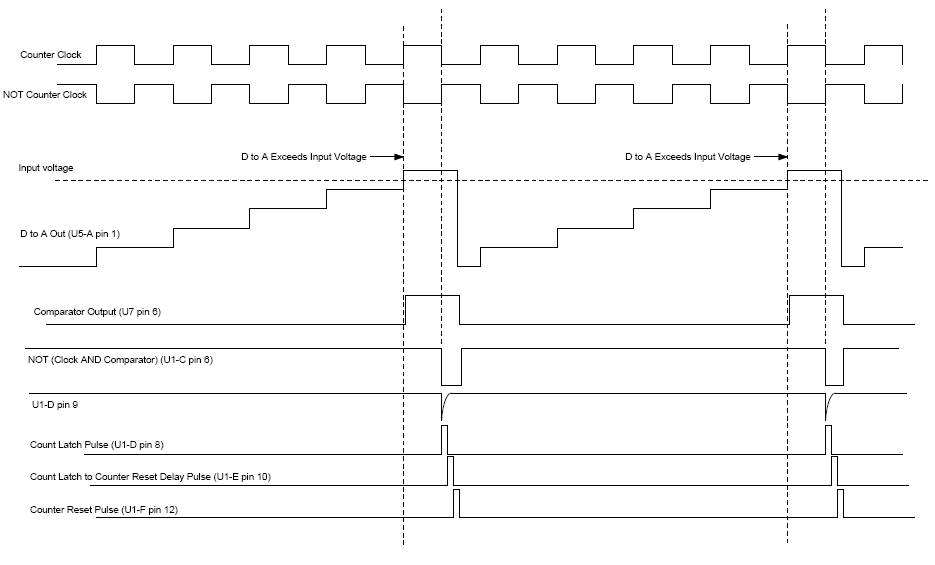
MFOS Voltage Quantizer Timing Diagram PDF
|
This timing diagram helps in the understanding of how the quantizer works. At the top you see the clock and NOT-clock waveforms. NOT-clock is actually the original clock output in this case. This is because U1-A's output is inverted by U1-B and it's output actually clocks the counters that form the comparator's reference D to A. So it's output is referred to as clock and U1-A's output is referred to as NOT-clock (since it is inverted from the counter driving clock). As you can see when the comparator reference D to A's voltage goes above the level of the input voltage the output of the comparator (formed by U7 and associated components) goes high. When it is high and NOT-clock goes high the NAND gate formed by D1, D2, R6 and U1-C goes low. The NAND operation is that the output of U1-C goes low when BOTH inputs (the cathodes of D1 and D2) are high simultaneously. That front end of that low transition is fed via C1 to the input of U1-D. R5 pulls the input of U1-D high again very quickly so that the output of U1-D is a very narrow pulse 2uS. As U1-D's output goes low its falling edge is fed via C3 into the input of U1-E which causes it to output a 2uS pulse. As U1-E's output goes low its falling edge is fed via C4 into the input of U1-F which causes it to output a 2uS pulse. U1-D's output pulse latches the current count into the 6 bit latch formed by U2 and U4. U1-F's output pulse resets the cascaded 8 bit counter (U3 and U6). U1-E functions as a delay generator to put 2uS between these pulses. This insures that the count has been safely stored in the latch before the counter is zeroed. |
| Approx. Current Consumption | |
| +12V | 11mA |
| -12V | 11mA |
| +15V | 12mA |
| -15V | 12mA |
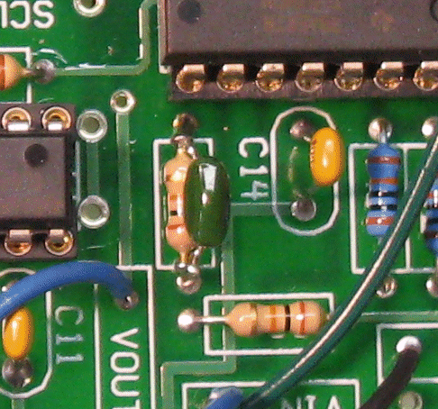
Kludging in the .01uF cap across R37.
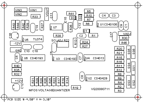
MFOS Voltage Quantizer PCB Parts Layout (Parts Side Shown) PDF
MFOS Voltage Quantizer PCB Parts Values (Parts Side Shown) PDF
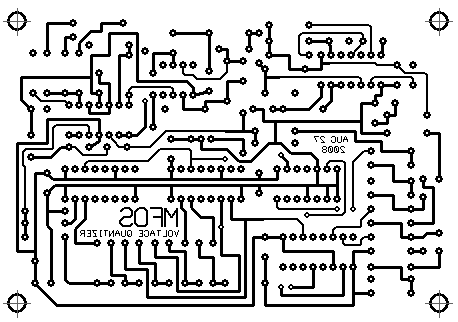
MFOS Voltage Quantizer PCB Bottom Copper (Parts Side Shown)
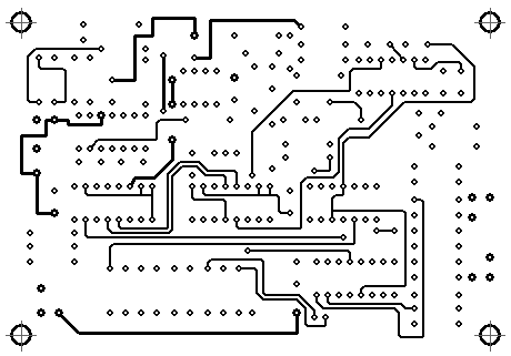
MFOS Voltage Quantizer PCB Top Copper(Parts Side Shown)
MFOS Voltage Quantizer PCB Top Silk Screen
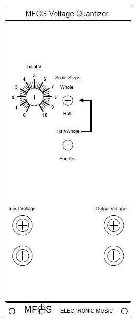
MFOS Voltage Quantizer Front Panel PDF
Ultra simple front panel. I made mine like this so I could put it into one of my prototype pre-made panels.
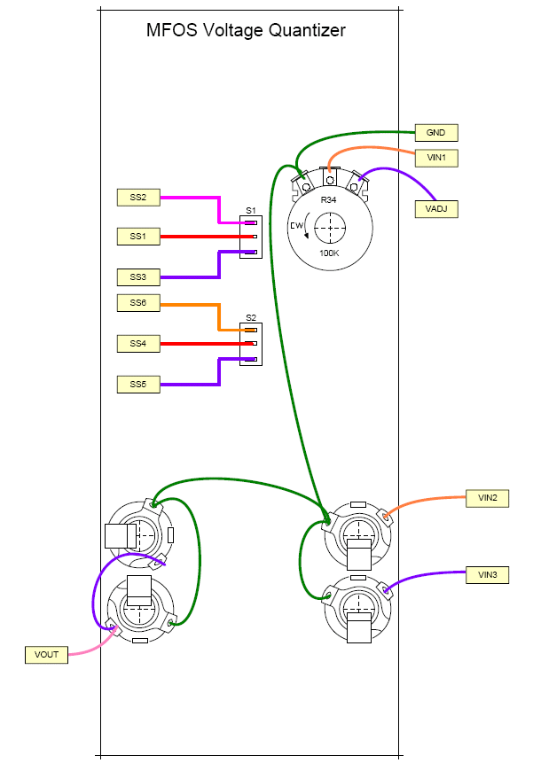
MFOS Voltage Quantizer Front Panel and Wiring PDF
Ultra simple front panel wiring.
MFOS Voltage Quantizer Project Parts List
Use precision metal film 0.1% tolerance for these resistors if you can find them at a reasonable cost.
Otherwise as I stated above hand pick them from 1% metal film resistors to find 0.1% tolerance parts.
Remember NOT to buy the corresponding resistors in the main list if you buy these.
| Qty. | Description | Value | Designators |
|---|---|---|---|
| 10 | 0.1% 100K Precision Metal Film Resistors | Resistor | R4, R12, R16, R21, R24, R18, R23, R26, R29, R32 |
| 17 | 0.1% 200K Precision Metal Film Resistors | Resistor | R2, R3, R8, R45, R9, R11, R15, R20, R27, R14, R19, R17, R25, R28, R31, R35, R40 |
MFOS Voltage Quantizer Project Parts List
| Qty. | Description | Value | Designators |
|---|---|---|---|
|
|
|||
|
|
|||
| 1 | TL071 Op Amp | TL071 | U7 |
| 1 | TL074 Quad Op Amp | TL074 | U5-B, U5-A, U5-C, U5-D |
| 1 | CD40106B Hex Inverter | CD40106 | U1-B, U1-C, U1-E, U1-F, U1-D, U1-A |
| 1 | CD4013B Dual D Flip Flop | CD4013 | U4 |
| 2 | CD40193B 4 Bit Counter | CD40193 | U3, U6 |
| 1 | CD4042B Quad Clocked D Latch | CD4042B | U2 |
| 3 | 1N914 Sw. Diode(s) | VALUE | D2, D1, D3 |
| 1 | Capacitor Ceramic(s) | .01uF | Kludge soldered across R37 |
| 10 | Capacitor Ceramic(s) | .1uF | C5, C6, C7, C9, C11, C8, C10, C14, C15, C17 |
| 4 | Capacitor Ceramic(s) | 100pF | C1, C3, C4, C2 |
| 1 | Capacitor Ceramic(s) | .002uF | C18 (Changed from 200pF to .002uF) |
| 2 | Capacitor Electrolytic(s) | 1uF | C16, C12 |
| 1 | Linear Potentiometer | 100K | R34 |
| 1 | Trim Pot | 10K | R22 |
| 14 | Resistor 1/4 Watt 1%(s) | 100K | R44, R42, R18, R23, R26, R29, R32, R24, R21, R16, R12, R4, R39, R43 |
| 1 | Resistor 1/4 Watt 1% | 10K | R38 |
| 18 | Resistor 1/4 Watt 1%(s) | 200K | R1, R45, R14, R19, R17, R25, R28, R31, R35, R40, R27, R20, R15, R11, R8, R2, R3, R9 |
| 5 | Resistor 1/4 Watt 1%(s) | 20K | R5, R7, R10, R37, R33 |
| 1 | Resistor 1/4 Watt 1% | 3M | R36 |
| 1 | Resistor 1/4 Watt 1% | 4.7K | R41 |
| 1 | Resistor 1/4 Watt 1% | 47K | R6 |
| 2 | Resistor 1/4 Watt 1%(s) | 75K | R30, R13 |
| 2 | SPDT Switch | SPDT | S1, S2 |
Miscellaneous
- 1/16" Thick aluminum plate for mounting the pots and switches.
- Unit is typically mounted in a synth case with other synth modules.
- Assorted hardware 1" 6-32 nuts and bolts, 1/2" #8 wood screws, etc
- Knobs for potentiometers, wire and solder.
- Digital Volt Meter and a Signal Tracer or oscilloscope for testing.