Ray Wilson authored this content while he was actively running MFOS as the founder and resident genius.
We retain the content because it reflects a valuable point of view representing that time and place.
Article by Ray Wilson
Features
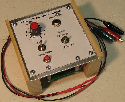
IntroductionThis is the volt per octave calibrator I developed to make calibrating VCOs and VCFs easier. I used this in the "MFOS VCO Calibration Part I" and "MFOS VCO Calibration Part II" YouTubes. It is way easier than constantly resetting a regular power supply and way cheaper than a programmable power supply.
|
 |
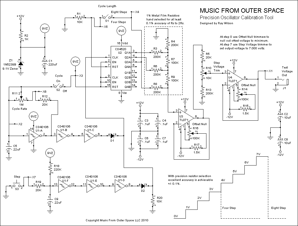
Volts Per Octave Calibrator Schematic Page 1 PDF
|
The circuit is fairly simple but does the job of providing a nice accurate 0 thru 7 volt source that steps by 1V increments. With careful selection of the resistors used in the R/2R ladder (R3,R4,R6,R7,R8,R9) you can get 0.1% accuracy. The circuit is powered by a simple zener supply so that the voltages used in the 1V stepping circuit don't depend too heavily on the supply voltage (+12V and -12V or +15V and -15V). You should be powering this from a stable source of voltage like your synth's supply or your bench supply. I ran the +V, -V, and Ground supply wires to alligator clips so I can just piggy back on whatever voltage I am feeding into whatever I am calibrating. Recalibrate the circuit any time you switch supplies. For example any time you go from +/-12V to +/-15V or +/-15V to +/-12V. We use a CD40106 (hex inverting schmitt trigger) to supply a free running clock source and a manual step clock source. U1-A,B, and C are used in the free running clock source. U1-A and R11, R12 and C5 comprise a square wave oscillator that goes from ground to 9VZ. U1-A's output is always reaching around to it's input and causing it to change state. With U1-A's output low C5 discharges (via R11 and R12) until it is below U1-A's lower trip point at which time U1-A's output goes high and then when C5 charges (via R11 and R12) to above U1-A's upper trip point U1-A's output goes low and the cycles continue to repeat. R12 in series with R11 (1 meg linear pot) supply rate control as they determine how fast or slow C5 charges and discharges. U1-B in conjunction with U1-C buffer U1-A's output. The high going excursions of U1-C's output forward bias D1 and drop 9VZ (minus a negligible diode drop) on R20. When the Cycle On/Off switch (S2) is open the square waves dropped on R20 are applied to the CLK input of counter A in the CD4520 Dual Binary Counter and it counts from 0 to 3 or 0 to 7 depending on the setting of S1. When the Cycle On/Off switch (S2) is closed 9VZ is applied to pin 1 of U1-A which stops the oscillation and causes U1-C to go to a low state. In this condition no clock pulses are applied to the CLK input of counter A in the CD4520 Dual Binary Counter and it is incremented by the manual step control only. U1-F, E, and D comprise the manual clock source. We use the hysteresis of the CD40106 to debounce the pushbutton. Normally with S3 open 9VZ through R18 charges C9 and hold U1-F and subsequenctly U1-D's output low. When S3 is pressed C9 is discharged via R19 to about ground causing U1-F and subsequenctly U1-D's output to go high providing a clock signal via D2 to be applied to U2's counter A CLK input. When the button is released C9 charges up again and U1-F's output goes low. The low pass filtering provided by the RC networks of R18/C9 and R19/C9 keep the switch chatter from causing multiple clocks to be emitted. S1 controls the maximum count U2 attains before resetting. With S1 closed the counter resets when Q3A goes high (count of 4) since the 4 count resets the counter it never gets to 4 but cycles 0 thru 3. With S1 open the counter cycles 0 through 7 repeatedly. Q1A, Q2A, and Q3A feed the R/2R network. As the counter counts from 0 through n the voltage picked off of the R/2R network steps up in equal increments. It is VERY IMPORTANT TO SELECT R3,R4,R6,R7,R8, and R9 to within +/-0.1% of the target values. You don't have to be exactly 100K and 200K you just need the R to 2R ratio to be consistent between them all. For example lets say you measure several resistors from the 100K 1% metal film batch you have and find two at 99.50K +/-0.1%. Set these aside and now as you go through the 200K batch you must look for 4 pieces that are 199.00K +/-0.1%. You see... the ratio of the values is important not the actual values. However do not think "Hey, I've got some 1K and 2K I can use..." We use 100K and 200K so as not to load the outputs of the CD4520 to make sure that the R/2R network gets nice pure 9VZ levels. U3 buffers the output of the R/2R ladder and supplies the buffered voltage to U4 via level trim network R5, R10 (trimmer), and R13. U4 then buffers the trimmed voltage and drives the output via J1. C2 and C8 clean up the power coming into the board and C3,C4,C6, and C7 are used to bypass the power supply close to the op amp power pins. Calibration We are going to measure the outputs of U3 and U4 to make sure they are "nulled" i.e. their outputs are as close to 0V as possible. Ensure that counter U2 is at step zero (Q1, Q2, and Q3 all low). As you observe the voltage on the output of U3 (pin 6) adjust trimmer R16 until you read as close to 0V as possible. As you get closer to 0V adjust your meter's range down to 200mV (or better) to get greatest precision as you get to the target 0V. Do the same for U4 using trimmer R14. Now ensure counter U2 is at step 7 (Q1, Q2, and Q3 all high). As you observe the output of U4 (pin 6) adjust trimmer R10 until you read as close to 7.000 volts as possible at the output of U4. You should now see that the steps are very close to 0,1,2,3,4,5,6 and 7 volts with high (+/-0.1%) accuracy. Changing Cycle Rate Range If you would like to slow the cycle rate range you can increase the value of C5. You can use ceramic caps or non-polarized aluminum caps or even aluminum or tantalum polarized caps but if you use a polarized cap make sure you put the negative side of the cap to ground. The ground side of the cap is the donut that also connects to U1 pin 7. I suggest keeping the value below 2uF but that's just a suggestion (larger values won't hurt anything). |
| Approx. Current Consumption | |
| +12V | 15mA |
| -12V | 15mA |
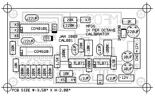
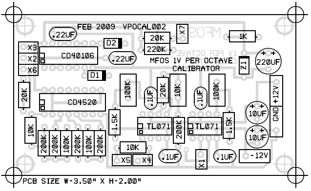
Volts Per Octave Calibrator PCB Component Values (Parts Side Shown) PDF
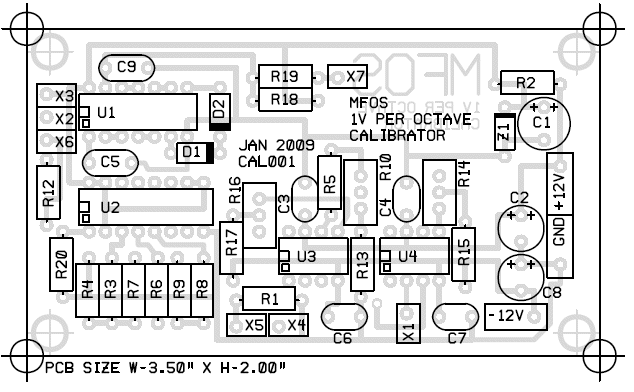
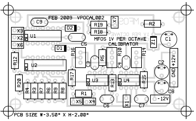
Volts Per Octave Calibrator PCB Component Designators (Parts Side Shown) PDF
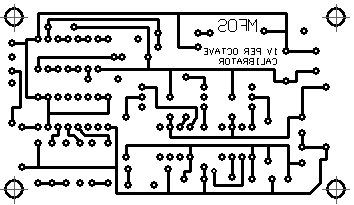
Volts Per Octave Calibrator PCB Top Copper(Parts Side Shown)
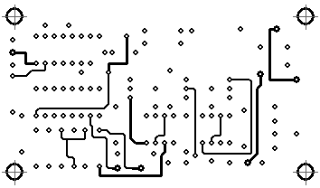
Volts Per Octave Calibrator PCB Top Silk Screen
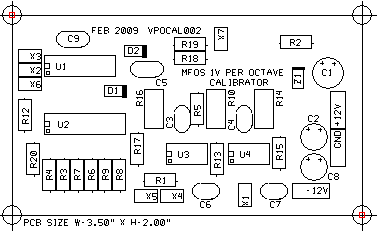
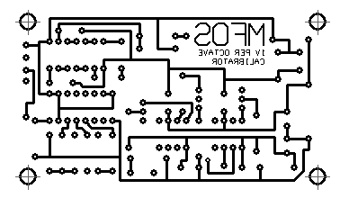
Volts Per Octave Calibrator PCB Top Copper(Parts Side Shown)
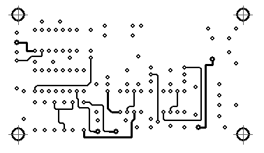
Volts Per Octave Calibrator PCB Top Silk Screen
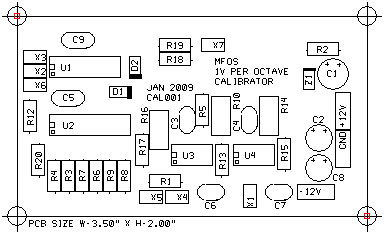
Volts Per Octave Calibrator PCB Populated
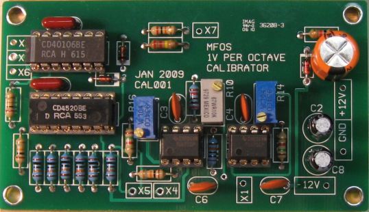
Mount the sockets first then add the cap afterwards.
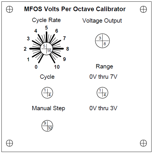
Volts Per Octave Calibrator Front Panel PDF
Just a suggestion to show which controls the front panel needs to support.
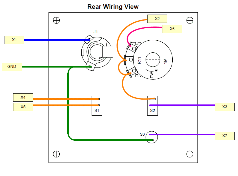
Volts Per Octave Calibrator Front Panel and Wiring Rear View PDF
Back view of the wiring for the suggested panel layout.
Volts Per Octave Calibrator Front Panel FPD
Sean Dynan of Ireland shared a 8 hp Euro panel layout. You need "Front Panel Express" to view it. I suggest you create a wiring diagram for yourself if you decide to use this layout.

Volts Per Octave Calibrator Project Parts List
| Qty. | Description | Value | Designators |
|---|---|---|---|
| 1 | CD40106 | CD40106 | U1 |
| 1 | CD4520 Dual Binary Counter | CD4520 | U2 |
| 2 | TL071 Op Amp | TL071 | U3, U4 |
| 2 | Diode 1N914 | VALUE | D1, D2 |
| 1 | Diode Zener | 1N5239B | Z1 |
| 2 | Cermet Multiple Turn Trim Pot | 100K | R14, R16 |
| 1 | Cermet Multiple Turn Trim Pot | 10K | R10 |
| 1 | Linear Potentiometer | 1M | R11 |
| 2 | Resistor 1/4 Watt 1% | 1.5K | R15, R17 |
| 2 | Resistor 1/4 Watt 1% | 100K | R7, R9 |
| 5 | Resistor 1/4 Watt 1% | 200K | R3, R4, R6, R8, R13 |
| 1 | Resistor 1/4 Watt 1% | 20K | R5 |
| 2 | Resistor 1/4 Watt 5% | 10K | R1, R20 |
| 1 | Resistor 1/4 Watt 5% | 1K | R2 |
| 2 | Resistor 1/4 Watt 5% | 20K | R12, R19 |
| 1 | Resistor 1/4 Watt 5% | 220K | R18 |
| 4 | Capacitor Ceramic | .1uF | C3, C4, C6, C7 |
| 2 | Capacitor Ceramic | .22uF | C5, C9 |
| 2 | Capacitor Electrolytic | 10uF | C2, C8 |
| 1 | Capacitor Electrolytic | 220uF | C1 |
| 2 | Switch SPST | SPST | S1, S2 |
| 1 | Switch SPST N.O. Push Button | SPST | S3 |
| 1 | Jack 1/4" 2 Terminal | Jack 1/4" 2 Terminal | J1 |
Miscellaneous
- 1/16" Thick aluminum plate for mounting the pots and switches.
- Unit is typically mounted in a synth case with other synth modules.
- Assorted hardware 1" 6-32 nuts and bolts, 1/2" #8 wood screws, etc
- Knobs for potentiometers, wire and solder.
- Digital Volt Meter and a Signal Tracer or oscilloscope for testing.

