Ray Wilson authored this content while he was actively running MFOS as the founder and resident genius.
We retain the content because it reflects a valuable point of view representing that time and place.
Article by Ray Wilson
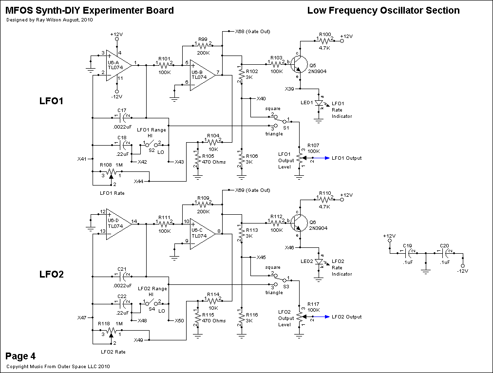
Low Frequency Oscillators Schematic (Page 4) PDF
The "Low Frequency Oscillators" are useful for modulating the CV of other modules on the Experimenter Board with either triangle or square waves. They are simple LFOs but function quite nicely and will give you another modulation source for your monster sound generator. When modulating (controlling the frequency of) the VCO for example with a low frequency triangle wave a siren type sound can be created. If the modulation range is set to high and the VCO is modulated a bell type timbre can be produced.
I am going to describe the operation of LFO1 located at the top of Schematic Page 4 Low Frequency Oscillator Section. LFO2 functions in exactly the same manner as LFO1 and thus it's operation will not be described.
The LFO oscillators are integrator/comparator type oscillators. An integrator is used to generate the triangle waveform and the comparator is used to both control the integrator ramp direction and to provide the square wave output of the LFO. A panel mounted LED is used to display the LFO's rate and there is a pot to control the amount of the LFO's output used to modulate the CV inputs of other modules. A switch allows selection of either square or triangle wave output and a high/low rate range control gives this LFO a very wide and useful frequency range.
U6-A is one of four op amps on the TL074 quad op amp chip. It and C17 function as an integrator whose output ramps up or down depending on the state of the output of U6-B. When U6-B's output is saturated high (about 1V below +V) current is fed to the non-inverting input of the integrator via R104 10K resistor and R108 1M panel mounted LFO1 Rate adjustment pot. By attenuating the voltage with R105 470 ohm resistor the overall rate of the LFO is lowered allowing use of smaller value integration capacitors. Current flowing into the integrator causes the output to ramp down until the output of U6-A goes below the lower trip point of comparator U6-B and associated components (R101 and R99). R101 100K resistor feeds the output voltage from U6-A to the non-inverting input of U6-B and R99 connected as a positive feedback resistor provides the hysteresis we need to get a nice +/-3.7V amplitude signal from U6-A. Once the integrator ramps down to about -3.8V the output of U6-B saturates low (about 1V above -V) immediately and current begins to be sucked out of the integrator (via R104 and R108) causing it's output to ramp up until it exceeds the positive trip point of comparator U6-B and associated components (R101 and R99). When the positive trip point voltage is attained at the output of U6-A the output of U6-B shoots high and the cycle repeats.
SPDT toggle switch S1 permits selection of either the raw triangle waveform (output of U6-A) or the square waveform (attenuated by divider R102 3K resistor and R106 3K resistor to ground) to be fed to the 100K output level set potentiometer R107. The wiper of R107 goes to the LFO1's front panel output jack. SPST toggle switch S2 allows C18 .22uF capacitor to be put in parallel with integrator cap C17 and reduces the frequency range of the LFO by a factor of about 100.
Additionally, when U6-B's output is high current is fed to the base of Q5 2N3904 NPN transistor via R103 100K resistor causing Q5 to turn on and allow current to flow through R100 4.7K resistor and light LED1. You can reduce the value of R100 if you prefer the LED to glow more brightly. I would not go lower than about 1K. When U6-B's output is low Q5 is biased off and the LED does not glow. Thus the LED flashes at the rate of the LFO. At high LFO rates the LED may appear to dim (go to half brightness).
X68 and X69 are the raw outputs of the comparators of LFO1 and LFO2 respectively. These circuit points can be used to externally gate the AR generators if you desire to connect them to a banana jack. By connecting the banana jack from the X68 or X69 circuit point to either AREG's external gate input you can cause it to repeat it's envelope at the rate set by the respective LFO1. Some interesting sonic effects can be achieved in this manner.
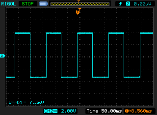
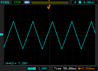
LFO Scope Photos
| Square Wave | Triangle Wave |
|
|
Low Frequency Oscillators PCB Parts Layout (Parts Side Shown)
I find this one useful for trouble shooting since the designators on the PC board are covered by the installed components.
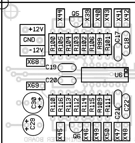
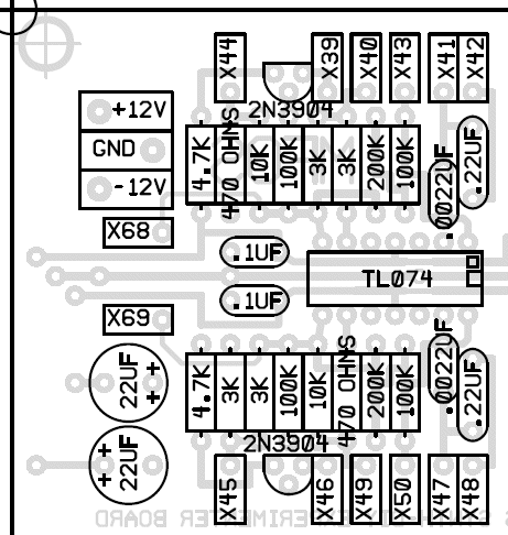
Low Frequency Oscillators PCB Part Value View (Parts Side Shown)
I find this one useful for populating the PC board since I don't have to continually refer back to the schematic to know the value for a designator.
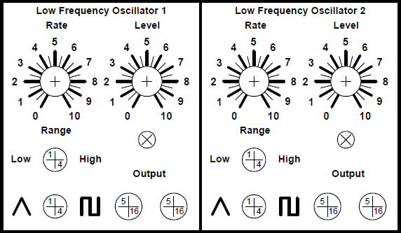
Low Frequency Oscillators Front Panel Template
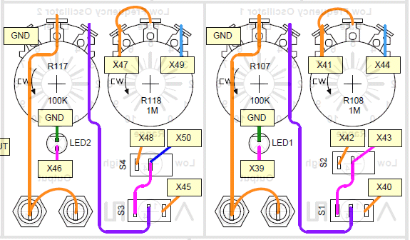
These front panel layouts are suggestions and are meant to illustrate the circuit's user interface and wiring between the panel and the PC board. I'm certain you can come up with a much cooler looking panel but this utilitarian version will certainly work to get you started.
Low Frequency Oscillators Front Panel Wiring
Low Frequency Oscillators Project Parts List
Resistor Color Chart For Resistors Used In This Circuit
The resistors should be carbon composition or carbon film.Use 1/4 watt resistors because 1/2 watt will be too big for the board.
| Qty. | Description | Value | Designators |
|---|---|---|---|
| 1 | TL074 Quad Op Amp | TL074 | U6 |
| 2 | 2N3904 General Purpose NPN Transistor | 2N3904 | Q5, Q6 |
| 2 | General Purpose LED | LED | LED1, LED2 |
| 2 | Potentiometer Linear Taper | 100K | R107, R117 |
| 2 | Potentiometer Linear Taper | 1M | R108, R118 |
| 4 | Resistor 1/4 Watt 5% | 100K | R101, R103, R111, R112 |
| 2 | Resistor 1/4 Watt 5% | 10K | R104, R114 |
| 2 | Resistor 1/4 Watt 5% | 200K | R99, R109 |
| 4 | Resistor 1/4 Watt 5% | 3K | R102, R106, R113, R116 |
| 2 | Resistor 1/4 Watt 5% | 4.7K | R100, R110 |
| 2 | Resistor 1/4 Watt 5% | 470 Ohms | R105, R115 |
| 2 | Capacitor Ceramic | .0022uF | C17, C21 |
| 2 | Capacitor Ceramic | .1uF | C19, C20 |
| 2 | Capacitor Ceramic | .22uF | C18, C22 |
| 2 | SPST Switch | SPST | S2, S4 |
| 2 | Switch SPDT | SPDT | S1, S3 |
Miscellaneous
- 1/16" thick aluminum plate for mounting the pots and switches.
- Assorted hardware 1" 6-32 nuts and bolts, 1/2" #8 wood screws, etc
- Knobs for potentiometers, wire, solder and typical assorted electronics hand tools.
- Digital volt meter and a signal tracer or oscilloscope for testing.