Ray Wilson authored this content while he was actively running MFOS as the founder and resident genius.
We retain the content because it reflects a valuable point of view representing that time and place.
Article by Ray Wilson
AR Envelope Generators Schematic (Page 5) PDF
The "AR Envelope Generators" are useful for modulating the CV of other modules on the Experimenter Board with an Attack Release type voltage envelope. They are simple AREGs but function quite nicely and will give you another modulation source for your monster sound generator. When modulating (controlling the frequency of) the VCO for example with an AREG envelope a chirping type sound can be created. When modulating (controlling the cutoff frequency of) the VCF for example with an AREG envelope a wah wah type sound can be created.
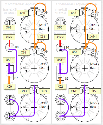
I am going to describe the operation of AREG1 located at the top of Schematic Page 5 AR Envelope Generator Section. AREG2 functions in exactly the same manner as AREG1 and thus it's operation will not be described.
The heart of the AR Envelope Generator is half of a CD4013 dual D flip flop. This IMHO is one of the most useful chips on the planet. We essentially set the CD4013 U8-B by applying a high level (basically V+) on it's SET line and then let the Q output wrap around after the envelope reaches it's peak voltage and reset itself by bringing the RESET line high by means of comparator U7-B and associated components. When the Q line falls low the R or Release phase begins and culminates in the complete discharge of C24.
With S5 (SPST Trig/Gate Mode) open (trig mode) and X56 not connected to anything (the typical state) pressing S6 causes a pulse to pass through C23 .01uF capacitor which is dropped across R122 100K resistor and the cathode of D3. When the switch is released C23 discharges quickly through R121 100K resistor. As C23 discharges it wants to pull U8-B pin 8 below ground due to cap coupling. D3 is used to clamp the voltage on U8-B pin 8 to one diode drop below ground to prevent possible damage to the chip. The positive pulse dropped on R122 100K resistor sets D Flip Flop U8-B causing it's Q output to go to a logic 1 (or V+). C24 which was initially discharged now begins to charge at the rate set by R119 470 Ohm resistor and R120 1M panel mounted Attack (time) potentiometer. When Q (U8-B pin 13) is high D1, 1N914 high speed diode, is forward biased allowing current to flow through it and R120 1M Attack (time) pot but D4, 1N914 high speed diode, is reverse biased so that the Decay pot setting does not affect the Attack time and vice versa.
U7-A is wired as a high impedance voltage follower (so it doesn't load C24) with negative offset and gain of 1.5. R127 47K feedback resistor and R126 100K gain set and bias resistor are used to set the gain and offset. R125 100K pot is used to adjust the level of the AR voltage envelope. R125's wiper is connected to the output jack of AREG1.
U7-B is configured as a high impedance comparator (so it doesn't load C24) with a trip voltage of about 6.8 volts. So when the voltage on C24 gets to about 6.8V it's output shoots high, forward biasing D5 and dropping V+ (minus a diode drop) on R123 100K resistor and bringing pin 10 of U8-B high resetting the D Flip Flop. When the flip flop is reset C24 discharges through R124 1M Decay (time) potentiometer, D4 (now forward biased) and R119 470 Ohm resistor. This results in a capacitive type charge curve followed by a capacitive type discharge curve the times of which are respectively set by R120 and R124. R119 serves as a current limiter minimum charge/discharge time setter. With the gain and offset provided by U7-A the envelope's output voltage goes from about -5V to about +5V.
When S5 SPST Trig/Gate Mode is closed and S6 is depressed a high voltage level is held on U8-B pin 8 so that even when the comparator (U7-B and associated components) goes high the Q output remains high until you release the switch. At that time the Q output goes low and the Release cycle is entered.
If it is desired to gate the AREG externally via X56 you must apply a pulse or step to X56 whose amplitude is close to +V of the power supply. The LFO can be used as a source of repeat gates as explained on the LFO page regarding circuit points X68 and X69.

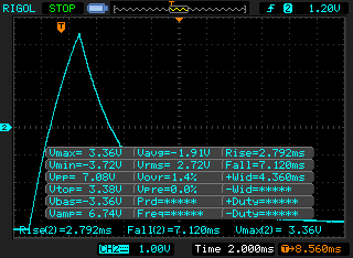
AREG Scope Photos
| Fastest Envelope (P to P voltage) | Fastest Envelope (w/measurements) |

|
|
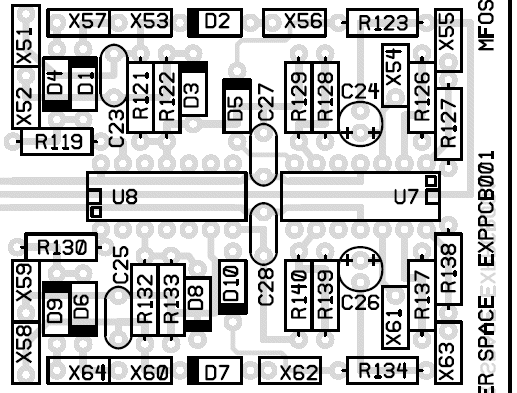
AR Envelope Generators PCB Parts Layout (Parts Side Shown)
I find this one useful for trouble shooting since the designators on the PC board are covered by the installed components.
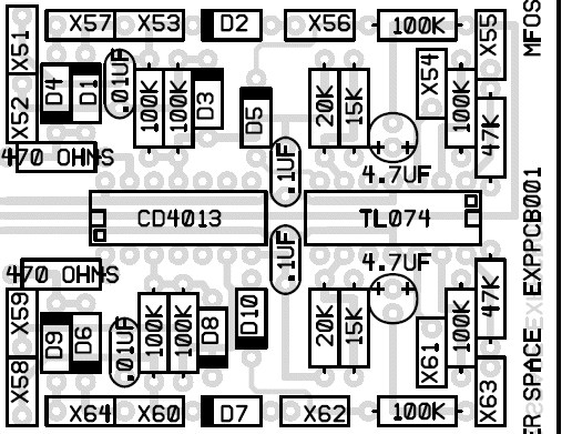
AR Envelope Generators PCB Part Value View (Parts Side Shown)
I find this one useful for populating the PC board since I don't have to continually refer back to the schematic to know the value for a designator.
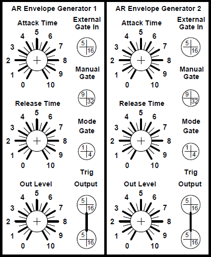
AR Envelope Generators Front Panel Template
These front panel layouts are suggestions and are meant to illustrate the circuit's user interface and wiring between the panel and the PC board. I'm certain you can come up with a much cooler looking panel but this utilitarian version will certainly work to get you started.
AR Envelope Generators Front Panel Wiring
AR Envelope Generators Project Parts List
Resistor Color Chart For Resistors Used In This Circuit
The resistors should be carbon composition or carbon film.Use 1/4 watt resistors because 1/2 watt will be too big for the board.
| Qty. | Description | Value | Designators |
|---|---|---|---|
| 1 | CD4013 Dual D Flip Flop | CD4013 | U8 |
| 1 | TL074 Quad Op Amp | TL074 | U7 |
| 10 | 1N914 Sw. Diode | 1N914 | D1, D2, D3, D4, D5, D6, D7, D8, D9, D10 |
| 4 | Potentiometer Audio Taper | 1M | R120, R124, R131, R135 |
| 2 | Potentiometer Linear Taper | 100K | R125, R136 |
| 8 | Resistor 1/4 Watt 5% | 100K | R121, R122, R123, R126, R132, R133, R134, R137 |
| 2 | Resistor 1/4 Watt 5% | 15K | R128, R139 |
| 2 | Resistor 1/4 Watt 5% | 20K | R129, R140 |
| 2 | Resistor 1/4 Watt 5% | 470 Ohms | R119, R130 |
| 2 | Resistor 1/4 Watt 5% | 47K | R127, R138 |
| 2 | Capacitor Ceramic | .01uF | C23, C25 |
| 2 | Capacitor Ceramic | .1uF | C27, C28 |
| 2 | Tantalum Capacitor | 4.7uF | C24, C26 |
| 2 | SPST Switch | SPST | S5, S7 |
| 2 | Switch SPST N.O. Push Button | SPST | S6, S8 |
Miscellaneous
- 1/16" thick aluminum plate for mounting the pots and switches.
- Assorted hardware 1" 6-32 nuts and bolts, 1/2" #8 wood screws, etc
- Knobs for potentiometers, wire, solder and typical assorted electronics hand tools.
- Digital volt meter and a signal tracer or oscilloscope for testing.