Ray Wilson authored this content while he was actively running MFOS as the founder and resident genius.
We retain the content because it reflects a valuable point of view representing that time and place.
Article by Ray Wilson
The MFOS Micro-Sample & Hold is a nice addition to your voltage controlled sound generator project whether it's a Synth-DIY Experimenter PC Board project, Sound Lab Mini-Synth or large modular synth project. It is as simple as a Sample & Hold can be yet features variable sample rate and output voltage glide (portamento). Its a simple way to add more flexibility to your synthesizer.
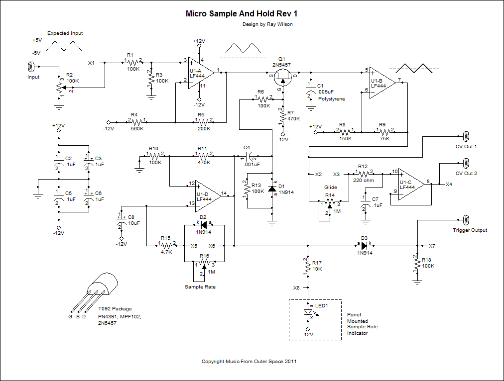
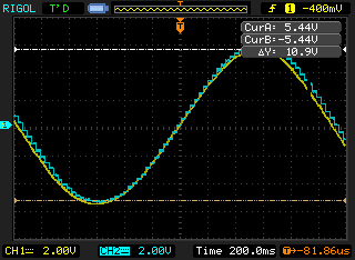
| Cursors highlight the level of the signal fed to circuit point X1 (yellow). Notice it can oscillate about ground. | Cursors highlight the level of the signal at U1-A pin 1. Notice it is level shifted to above ground and also attenuated by the resistor divider R1 and R3. |
 |
 |
Q1 N-Channel JFET 2N5457 acts like a closed switch (between source and drain) when it's gate is brought slightly above ground by differentiated pulses which are generated by picking off the front end of the rectangle wave output by U1-D sample clock generator. Normally (when no pulse is being applied) the gate of Q1 is held at about -3.6V by resistor network R7, R6 and R13. The voltage that is present at the source of Q1 passes through to the drain and charges (or discharges as the case may be) C1 where the sampled voltage is held until the next pulse hits the gate. U1-B buffers the sample held on the cap. The LF444CN chip has ultra low input current which allows the sample to sit on the cap and be buffered by U1-B for quite some time. With no pulse applied to the gate of Q1 it essentially acts like an open switch (source to drain) and the voltage on C1 does not leak back through the transistor. Buffer U1-B applies gain of about 1.5 and also level shifts the signal so that it approximates the original input level and oscillates about ground.
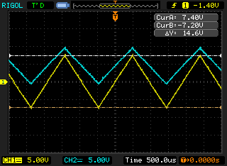
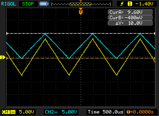
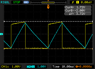
| This is the sampled and held voltage (blue) as it compares to the input voltage (yellow). Notice the level is shfted so that it reflects the actual input signal level. | Another shot of the sampled voltage. This is a lower frequency sine wave and a high sample rate. | This is the differentiated pulse that is applied to the gate of Q1 via C4 in series with R6. Q1 source to drain is essentially a closed switch during the pulse. The output changes during the pulse as a new sample is acquired. |
 |
 |
 |
Sample clock generator U1-D and associated components works as follows. If we begin our analysis imagining that the output of U1-D just went low (to about -11V) we see that the voltage level applied to U1-D pin 12 is about -1.9 volts. C8 (10uF aluminum or tantalum electrolytic capacitor) which had previously been charged (remember U1-D just went low and was high prior to that transition) to well above ground (actually to about 2V) begins to discharge via R15 and 1M Sample Rate adjust pot R16. When C8 discharges to below -1.9 volts (the level on pin 12 remember) the output of U1-D shoots to about +11V causing the voltage at U1-D pin 12 to go to about +1.9V and also causing C8 to charge from it's previous voltage (about -2V) towards V+ via D2 (1N914 high speed diode) and R15 (4.7K resistor). When C8 charges to above the level on U1-D pin 12 (about +2V), U1-D's output shots low again and this cycle continues. The output of U1-D is an asymmetric rectangular pulse wave due to D2 which allows the positive excursion of U1-D to charge C8 without the effect of 1M Sample Rate pot R16. Thus the high time is limited to about 20 mS and the low time depends on the setting of 1M Sample Rate pot R16. The rate of the sample clock can be varied from about 0.33 hertz to about 30 hertz. The sample clock's output is fed through D3 (1N914) and dropped on R18 (100K resistor) and then connected to the jack for the trigger output.
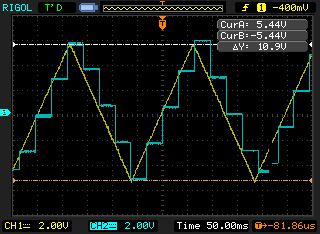
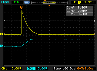
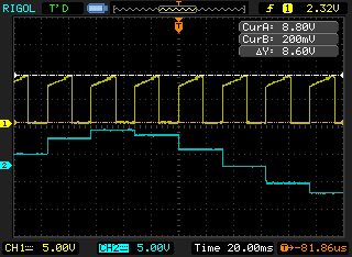
| These are the signals observed on the inputs of U1-D. The blue waveform is the charge and discharge of C8 on U1-D pin 13. The yellow waveform is the voltage seen on pin 12. It is a mini-me version of the output seen on U1-D pin 14. | This is the trigger output (yellow) and the sampled voltage (blue). The LF444CN's output has a bit of a hard time driving 2mA through the LED but works fine and is within the op amps operational parameters. Use a high efficiency LED for best results. The circuit drives a general purpose LED just fine IMHO. |
 |
 |
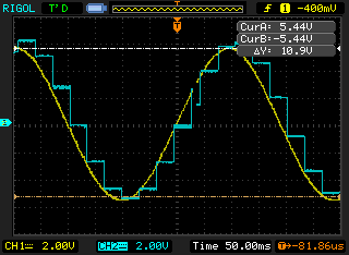
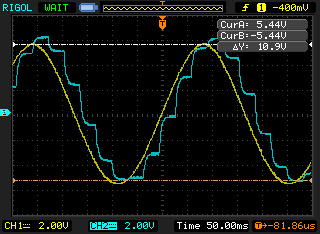
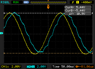
The output of U1-B feeds the CV Out 1 banana jack (or whatever jack you use) and also is input to the glide circuit comprised of U1-C and associated components. R14 (1M audio taper pot) in series with R12 (220 ohm resistor) is used to adjust the charge and discharge time of C7 (glide effect). The high input impedance of U1-C simply buffers the voltage on C7. The scope photos show the effect of adjusting R14 from no glide to more and more glide.
| With no glide the output of U1-C steps from level to level just about immediately. | With more glide the voltages slew from one to the other. | With even more glide the voltages slew from one to the other more slowly. |
 |
 |
 |
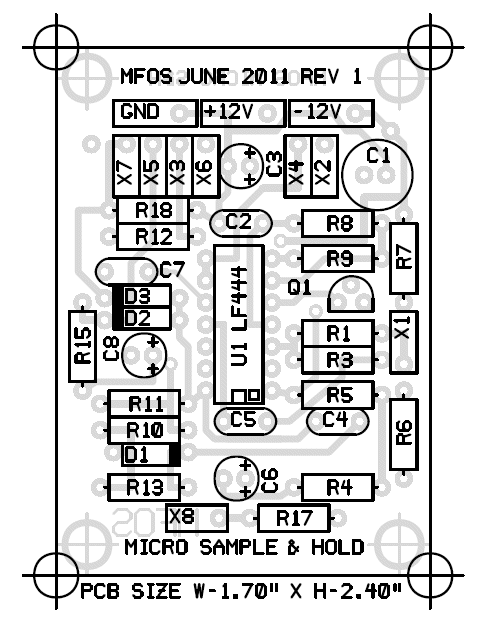
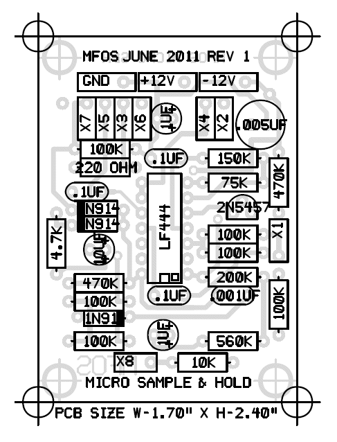
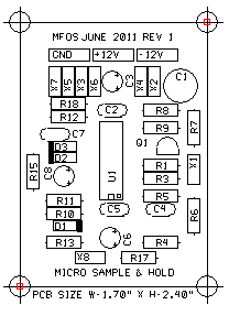
Micro Sample & Hold Board Details
| Micro Sample & Hold PC Board Parts Legend | Micro Sample & Hold PC Board Parts Values The diodes are 1N914 (the 1 and 4 are obscured in the image). |
|
 |
 |
|
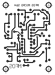
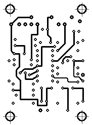
| Bottom Copper | Top Copper | Silk Screen | |||
 |
 |
 |
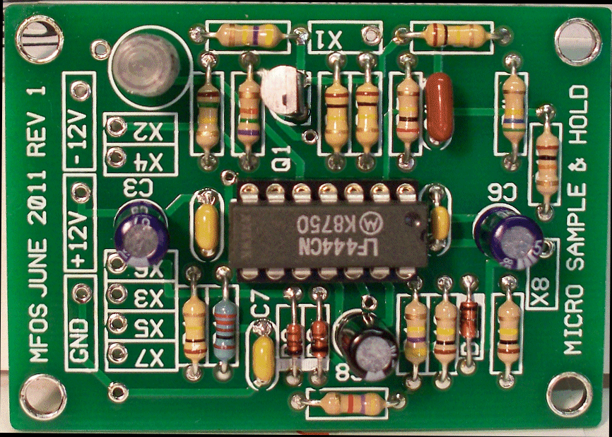
Micro Sample & Hold Populated (click for larger image)
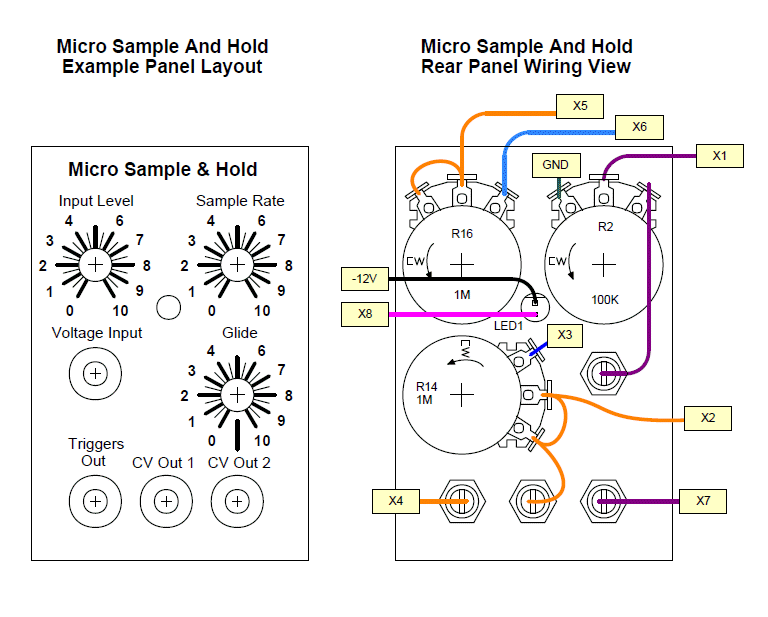
Micro Sample & Hold Panel Example And Wiring Diagram
Here are the essential details to wiring the Micro Sample & Hold to a panel for stand-alone operation. It makes a great modulation source for the Synth-DIY Experimenter Board, the Sound Lab Mini-Synth or your modular synth.
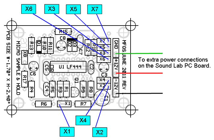
Micro Sample & Hold Sound Lab Plus Panel Connections
Here are the essential details to wiring the Micro Sample & Hold to the Sound Lab Mini Synth Plus.
Micro Sample & Hold Project Parts List
| Qty. | Description | Value | Designators |
|---|---|---|---|
| 1 | LF444 Quad Op Amp | LF444 | U1 |
| 1 | 2N5457 N Channel JFET | 2N5457 | Q1 |
| 3 | 1N914 Diode | 1N914 | D1, D2, D3 |
| 1 | General Purpose LED | Red LED | LED1 |
| 1 | Linear Taper Potentiometer | 100K | R2 |
| 1 | Linear Taper Potentiometer | 1M | R16 |
| 1 | Audio Taper Potentiometer | 1M | R14 |
| 6 | Resistor 1/4 Watt 5% | 100K | R1, R3, R6, R10, R13, R18 |
| 1 | Resistor 1/4 Watt 5% | 10K | R17 |
| 1 | Resistor 1/4 Watt 5% | 150K | R8 |
| 1 | Resistor 1/4 Watt 5% | 200K | R5 |
| 1 | Resistor 1/4 Watt 5% | 220 ohm | R12 |
| 1 | Resistor 1/4 Watt 5% | 4.7K | R15 |
| 2 | Resistor 1/4 Watt 5% | 470K | R7, R11 |
| 1 | Resistor 1/4 Watt 5% | 560K | R4 |
| 1 | Resistor 1/4 Watt 5% | 75K | R9 |
| 1 | Capacitor Alum. Electrolytic | 10uF | C8 |
| 2 | Capacitor Alum. Electrolytic | 1uF | C3, C6 |
| 1 | Capacitor Ceramic | .001uF | C4 |
| 3 | Capacitor Ceramic | .1uF | C2, C5, C7 |
| 1 | Capacitor Polystyrene Radial Leads | .005uF | C1 |
| 4 | Banana Jacks | ||
| 3 | Pot Knobs |