Ray Wilson authored this content while he was actively running MFOS as the founder and resident genius.
We retain the content because it reflects a valuable point of view representing that time and place.
Article by Ray Wilson
This is an intermediate to advanced project and I do not recommend it as a first project if you are just getting started in synths or electronics. Only the circuit and some explanation are shown here. A lot of project building, troubleshooting and electronics experience is assumed. Additionally, electronic equipment ownership (scope, meters, etc.) is taken for granted. If you are interested in building this project please read the entire page before ordering PC boards to ensure that the information provided is thorough enough for you to complete the project successfully.
Introduction
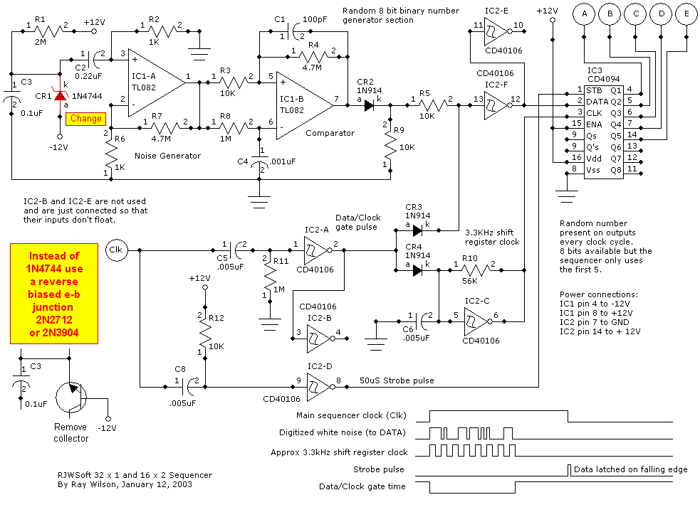
The main idea of a sequencer is to provide an automatic means of sequentially stepping through a series of adjustable voltages to drive a VCO (or any other voltage controlled device). Additionally, gate and trigger signals are generated at the moment the output of the circuit steps to a new voltage. Typically you use a sequencer to control the frequency of an oscillator (or several oscillators) to produce repeating tonal patterns, or arpeggios, which are further enhanced by filtering, modulation, addition of keyboard voltage etc. Sequencers are often used in electronic music production. This sequencer can produce a 32 note sequence or 2 parallel 16 note sequences. Additionally, this sequencer provides forward only, forward and back, and the unique ability for random sequencing.Schematic Page 1
Schematic Page 1 shows a very cool circuit that generates random 8 bit numbers. The sequencer only uses 5 bits output from IC3 (CD4094 8 bit shift register) but you could use this circuit a million different ways. For instance as a random voltage generator by hanging an R-2R ladder off of the CD4094's outputs. You would get 255 different volt steps. 12V divided by 255 equals steps of 47 mV which is a little over a half of a note when 1V/Oct equipment is in use. That's 12 octaves of semitones which is pretty cool and there will be no droop as in an analog switch and capacitor type sample and hold. I may build this later.
Noise is generated by IC1-A and associated components (notably the 1N4744 zener) the noise created at the reverse biased junction of CR1 is amplified by IC1-A. The noise signal is fed into the non-inverting input of IC1-B via R3 and the average value of the noise (due to filtering by R8 and C4) is fed into the inverting input of IC1-B which is configured as a comparator. When the voltage at pin 5 is slightly above the voltage seen at pin 6 the output (pin 7) shoots high. When the voltage at pin 5 is slightly below the voltage seen at pin 6 the output (pin 7) shoots low. R4 provides a slight bit of hysteresis and C1 causes the output to snap high and low. IC1-B's output (pin 7) is fed into IC2-F's input (pin 13) via CR2 and R5. CR2 permits only the positive excursions of IC1-B to drop across R9. These are presented to IC2-F pin 13, R9 pulls IC2-F pin 13 low during the blocked negative excursions. IC2-F further squares up and cleans the positive and negative transitions so that a serial stream of ones and zeros is presented to the DATA input of IC3 whenever the output of IC2-A is low. The sequencer's main clock signal appears at point Clk. The rising edge of clock passes through C5 and is dropped across R11. This pulse is squared up and inverted by IC2-A resulting in a 4 to 6 mS negative going pulse every clock cycle at the output of IC2-A. While the output of IC2-A is high diodes CR3 and CR4 permit current to flow to the inputs of IC2-F and IC2-C and thus present a high logic level at these inputs resulting in IC2-F's and IC2-C's outputs both being low. During the pulse time (when IC2-A's output is low) both diodes are reverse biased and IC2-F's input is allowed to follow the voltage dropped across R9 and IC2-C is permitted to oscillate. IC2-C oscillates because it is an inverting schmidt trigger and its output is fed back to its input via R10. IC2-C's output causes C6 to charge to 2/3 supply via R10 and then IC2-C pin 6 goes low and C6 discharges to 1/3 supply causing IC2-C's output to go high and the cycle repeats resulting in approximately 3KHz oscillation. You can see that the CD40106 is a very versatile chip to have around. The negative edge of Clk pulls IC2-D's input low momentarily via C8 (until R12 charges C8 back up) which results in a high pulse of approximately 50 uS at the output of IC2-D. The trailing edge of this pulse latches a new number into IC3's output latches. The sequencer's gate signal is an inverted version of this clock so a new random value is ready to go 50uS after the gate starts. The upshot of the whole thing, as you can see by the timing diagram, is that every clock cycle the shift register sees about 10 to twelve clocks on its clock input at the same time that digital noise is presented to the DATA input. Each clock of IC2-C shifts the random 1 or 0 present at DATA into the shift register. Finally at the falling edge of clock a strobe pulse is generated and presented to the shift register's strobe input so that the number sitting in the shift register's internal registers is latched into its output latches and appears at outputs Q1 thru Q8.
Construction and Testing Notes
- These instructions assume you are using internal clock (in case you have modified the design to include selectable external clock).
- Pin 12 of IC7-B should go low in response to pressing S9 (Start) momentarily.
- When R54 (Clock Rate) is set for highest rate (R54 essentially shorted) clock signal should appear at pin 12 of IC13-F.
- Clock should appear at pin 10 of IC13-E.
- Pin 6 of IC13-C should go high in response to pressing S12 (Step) and return low when it is released.
- Press S10 (Stop) and pin 12 of IC7-B should go high.
- Repeatedly pressing S12 (Step) should result in corresponding gates and triggers appearing at J5 and J6 respectively.
- Press S9 (Stop) and pin 12 of IC7-B should go low.
- Gates and triggers should appear at J5 and J6 respectively at the rate set by R54 (Clock Rate)
- DO NOT PRESS STOP because the following tests assume clock is running.
- Constant white noise should appear at pin 1 of IC1-A.
- Constant digitized noise should appear at the junction of CR2's cathode and R9.
- Gated digitized noise should appear at pin 2 of IC3.
- Gated 3KHz clock (approximate) should appear at pin 6 of IC2-C.
- The outputs of IC3 (points A,B,C,D and E) should be changing from one to zero in a non-cyclic fashion.
- Read the circuit description to understand what the LEDs should be doing in the various modes of operation.
- PRESS STOP because the following tests assume the clock is not running.
- While in various modes of operation use the Step switch (S12) to step the sequencer along.
- When an LED is lit its corresponding voltage adjust pot should be actively adjusting the voltage seen at the output jacks J1 thru J4 depending on the current mode of operation.
- Test that when you select a different voltage range (Hi, Low, and Mid) that the output voltage reacts accordingly.
- Hi should give 0V to 12V, Mid should give 0V to 6V and Low should give 0V to 3V (approximately).
- Always make sure that you have S5 set to No Reset when running in random mode. Not setting it will not harm the circuit but when the count randomly hits the one used to reset the sequence you get a momentary fight between zero and the current count causing two LEDs to look lit.
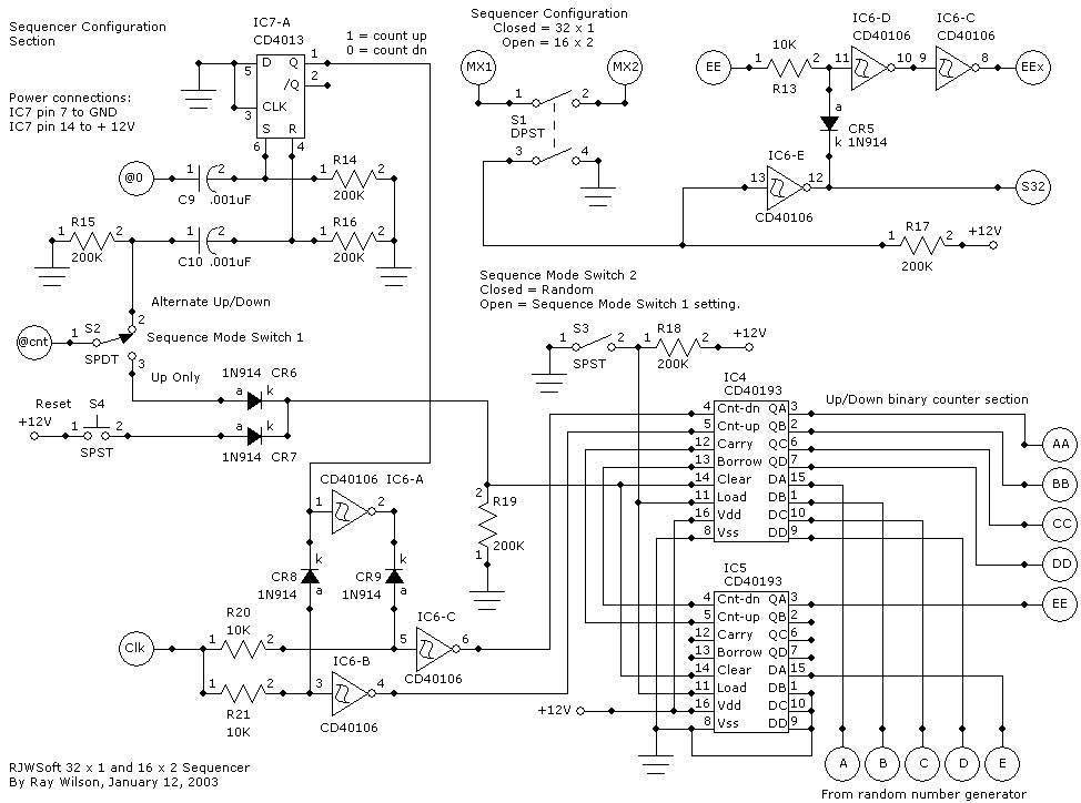
Schematic Page 2
Schematic Page two shows the circuitry that controls the sequencing mode. I will explain it switch by switch.
S2 is used to switch between "Up Only" mode and "Alternate Up/Down" mode. In "Alternate Up/Down" position the rising edge of @cnt (at count) which occurs when the sequencer has stepped to the terminating output (set via switches S5, S6 and S7 from Schematic Page 3) is presented to the Reset input of IC7-A (dual D flip flop) via C10 causing its Q output to go low. This output controls which clock input of IC4 (Up or Down) receives clock pulses. IC4 in conjunction with IC5 comprises a pre-loadable 8 bit up/down counter. When IC7-A's Q is high, clock pulses are permitted to pass from Clk via R21 into the input of IC6-B and on (after inversion) to pin 5 of IC4. The high on pin 1 of IC6-A causes a low at its output. This low allows current to flow through CR9 so that the clocks arriving at pin 5 of IC6-C via R20 are clamped to around 600mV. Since this voltage is always well below 1/3 of supply IC6-C's output is held high. This is exactly what we need since IC4 needs to have the Cnt-dn input held high while clocks are applied to Clk-up input. When IC7-A's Q output is low the opposite happens and IC4 counts down. IC7-A's Q goes high in response to the @0 pulse which occurs when the sequencer counts down to 0 and goes low in response to the @cnt pulse. The result is that the sequencer bounces up and down between 0 and the terminating output. When S2 is in "Up Only" mode the @cnt simply resets the CD40193 counters so that they keep going from 0 to the terminating count.
S4 just resets the counters to 0 when pushed.
S3 is used to switch between the two counting modes and random mode. In random mode the load inputs of IC4 and IC5 are held low which allows the data presented to the DA through DD inputs to be passed through to the QA through QD outputs. In this mode the random binary number (Points A through E From random number generator) control which sequencer output is active.
S1 does two things: it shorts points MX1 and MX2 (talked about during the Schematic Page 4 explanation) and it brings pin 13 of IC6-E low. When pin 13 of IC6-E is held low its output is held high which causes point S32 to be high and permits pin 11 of IC6-D to follow the voltage presented to point EE via R13. The logic level at this point appears at pin 8 of IC6-C. When S1 is open and IC6-E's input is held high via R17 to +12V, then IC6-E's output is held low which places a low on point S32 and clamps pin 11 of IC6-D so that its input never goes above 600 mV which results in a low being presented at point EEx. Point EEx and Point S32 are used to switch the sequencer's output generators (IC8 and IC9 on Schematic Page 3) from parallel 16 mode to serial 32 mode (and visa versa). This is accomplished by IC10 (CD4070 quad XOR gate) which controls the inhibit inputs of two CD4514 4 line to 16 line decoders. When S32 is held low then pin 4 of IC10-B is also held low and both CD4514s are enabled allowing them to act as two 4 to 16 line decoders in parallel. But, when S32 is held high then pin 4 is an inverted version of pin 5's logic level and the two CD4514s together act as a 5 line to 32 output decoder.
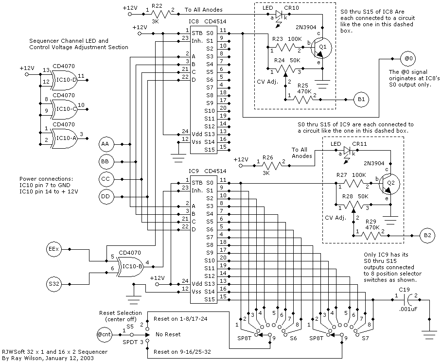
Schematic Page 3
Schematic Page 3 shows the CD4514s used as the sequencer output drivers, switches S5, S6 and S7 (used to select the terminating count), and the LED and voltage adjustment pot wiring. I use the 2N3904s to drive the channel indicator LEDs to avoid loading the outputs of the CD4514s. The outputs of the CD4514s go high when the corresponding binary count is present at the A through D inputs. Thus 0000 = S0 high, 0001 = S1 high, 0010 = S2 high, through 1111 = S15 high. If the Inh. (inhibit) input is held high the outputs are all forced to their low state irrespective of the data at A through D. The operation of IC10-B is explained above. C19 is glitch removal cap. During testing I noticed that when I selected S15 as the terminal count I was getting a reset on the 8 count. I could find no explanation of why this should be but there was an unmistakable glitch on the S15 line at count 8. It was so fast that it was at the edge of my scope's ability to see it (unfortunately the CD40193s saw it as plain as day). Anyway, C19 effectively casts this little gremlin to the ground (pun intended).
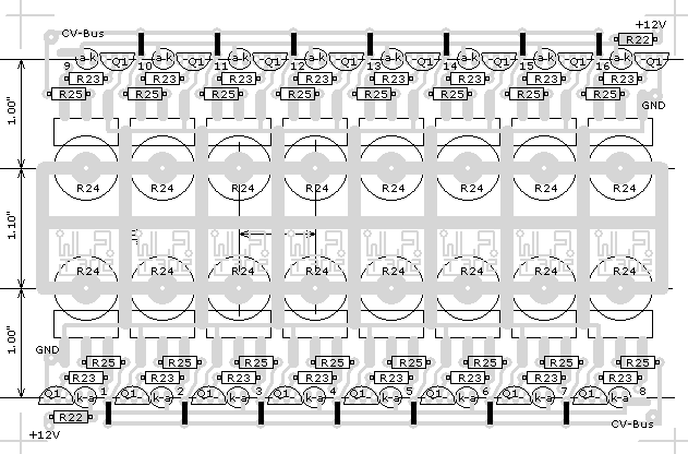
The outputs of the CD4514s are connected to their individual LED driver transistor's base via a 100K resistor and dropped across their individual voltage adjustment pot. Since only one LED is ever on at a time R22 feeds all of the anodes for IC8's indicator LEDs and R26 feeds all of the anodes for IC9's indicator LEDs. The wiper of each voltage adjustment pot feeds a summing resistor which is connected to a bus and fed to the inverting input of an op-amp (points B1 and B2 Schematic Page 4). There is a summing amp for IC8's outputs and one for IC9's outputs (Schematic Page 4).
S5 is used to choose between a terminal count between 1 and 7 or between 8 and 16. When it is set to center off the sequencer always goes to the last possible count (16 or 32).
Notice that this Schematic Page shows the origins of both: @0 and @cnt. The reason that I only use CD4514 IC9 to control the terminal count is this. If you want counts between 2 and 15 use the sequencer in parallel mode, if you want counts between 16 and 32 use it in serial mode. In my construction I came up with a circuit board to hold the circuitry you see in the dashed boxes. This is a good idea although you don't have to use the board I designed. Mine is designed to work with miniature pots. Design one that accomodates your pots and LEDs. Using a board reduces the number of wires you have to actually run when building this beast. Even with the circuit boards I'm still running well over 48 wires to accomodate the connections from the board to the mini-boards and to the terminal count switches. Better yet design it to work with DIP connectors and you could use cables with DIP plugs on them instead of all that messy wiring.
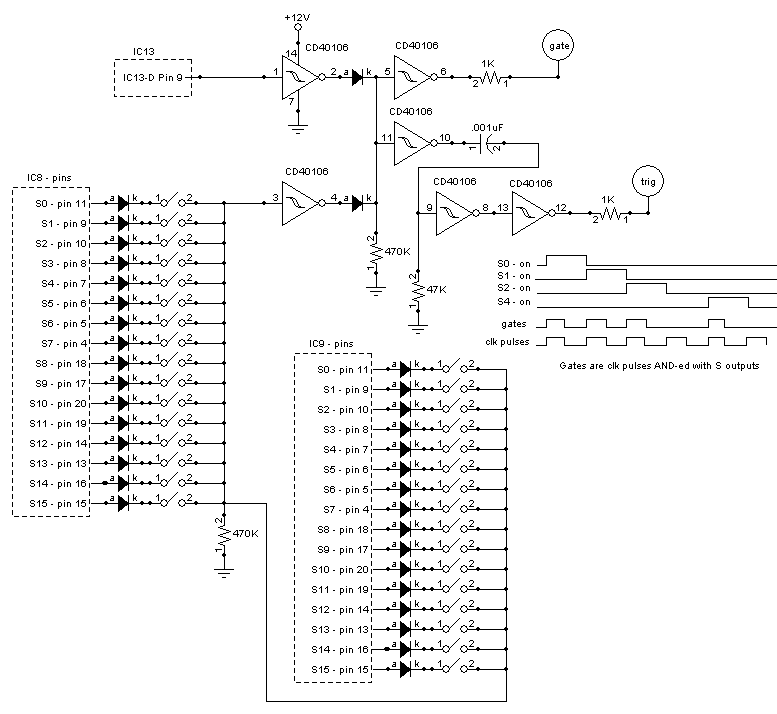
Gate Switch ModificationHere are some ideas that will help you add a gate switch for each output to control whether a gate occurs when the sequencer steps to that channel. THIS IS NOT ON THE CIRCUIT BOARD LAYOUT. If you want to add this you need to somehow kludge it into the existing circuit. Essentially when a switch is on the channel logical high is anded with the clock and the resulting gate lasts for the high period of the clock. If you notice that you are getting glitches (small logic spikes at the end of a channel's high time) add a small value cap from the gate or trigger output to ground (100 pF to .001uF should eliminate them). You don't have to add all of the diodes and switches. You can add them for one chip or the other or only for eight of one chip, etc. Experiment. | |
|
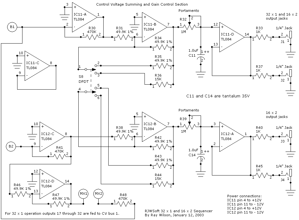
Schematic Page 4
This Schematic Page shows the summing op-amps for the adjustable voltages and the gain control op-amps. S8 simply changes the feedback resistance of IC11-B and IC12-B so that the voltage adjustment pots deliver: 12, 6 or 3 volts (approximately) depending on the setting of S8. The points MX1 and MX2 are shorted by S1 when in 32x1 output mode. During counts 0 through 15, the voltage from IC8's associated voltage adjustment pots is summed by IC11-A. The voltage from IC9's associated voltage adjustment pots is summed by IC12-C, inverted by IC12-D and fed via R48 to the summing point for IC8. Thus when in 32x1 output mode the voltages for all 32 channels appear on J1 and J2. In 32x1 mode during the 1 to 16 sequence 0 volts appears at J3 and J4, during the 17 to 32 sequence the voltages from the 17 to 32 pot settings appear at J3 and J4. In 16x2 mode the sequencer operates like two sequencers being controlled by the same counter and clock. The voltages from adjustment pots 1 to 16 appear at J1 and J2 and the voltages from adjustment pots 17 to 32 appear (at the same time) at J3 and J4.
Schematic Page 5
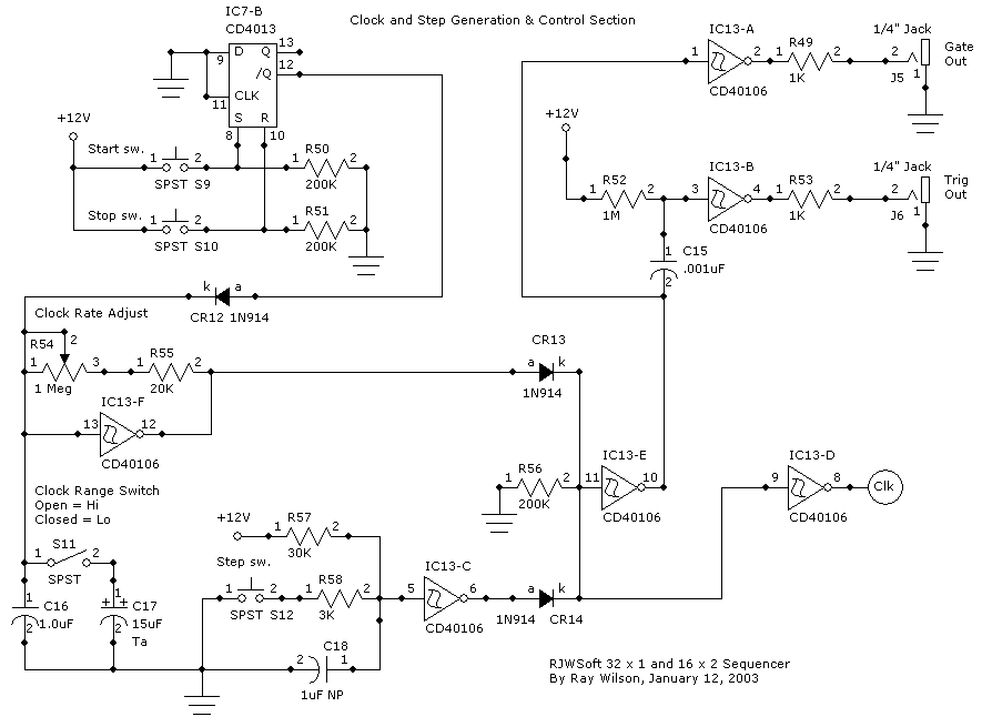
Schematic Page five shows the logic to start and stop the sequencer clock via pressing S9 or S10 respectively and the debounced step switch S12. R54 sets the sequencer's clock rate and S11 switches in more capacitance for really low clock rates. There is some overlap between the high and low rates. The gate and trigger outputs are generated so that they occur when the sequencer's voltage is changing.
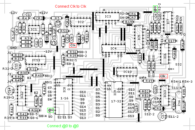
PCB Parts Layout for Sequencing Circuitry
As the red and green letters say: Connect Clk to Clk and @0 to @0 or nothing will work. I generally start by inserting all of the jumpers, then the sockets, then the resistors, then the diodes, then the caps. Also be careful when you are wiring the outputs. If you or I were laying out this chip I'll bet we would have put the outputs IN ORDER but it seems that the CD4514 designer was either dyslexic or very confused regarding the order of the arabic numeral system. In any case be very conscientious while wiring the outputs or your sequencer will be as whacky as the pinout.
Notice that in the upper left quadrant of the circuit board you see 4 caps that do not have numeric designators. The skinny ones are 0.1uF ceramic (or polyester) caps and the round ones are 1 to 10uF Electrolytics (Aluminum or Tantalum). They are power supply bypass caps.
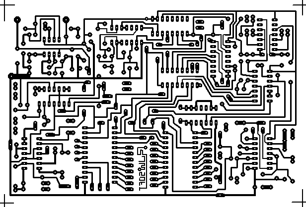
PCB Layout for Sequencing Circuitry (Parts Side Shown)
After etching watch for shorts wherever the traces are the closest (around IC2, IC6 and IC7). You might want to leave yourself more room around the edges for mounting the board.
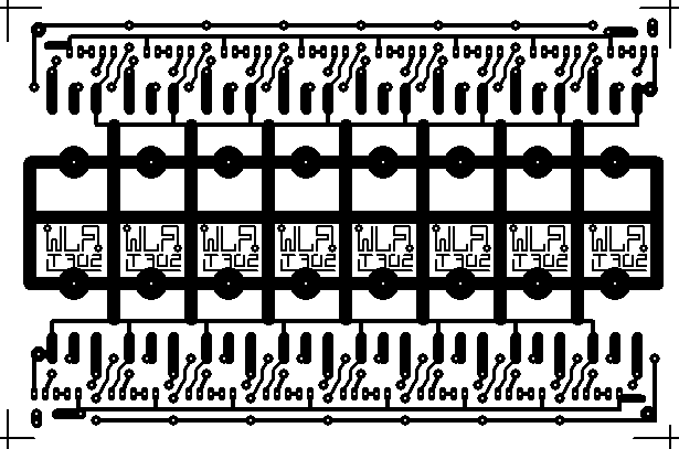
PCB Parts Layout for Pot and LED Boards
This is here to give you an idea of what I mean when I say make a PCB to hold the LED driver transistors, pots and associated circuitry. You need to make two of these. This board is sized for the smaller pots (they have an approximate 0.6 inch diameter). The pot is actually mounted with the body on the copper side and the lugs bent up to make contact with the copper (where they are tack soldered). The remaining components are mounted normally. Note that you only need one of the anode feeding resistors on each board and you can run a wire to connect the anode buses. I suggest that the pot shells be grounded somehow. You may want to configure your pots entirely differently to reduce 60 cycle noise etc but this is my prototype.
PCB Layout for Pot and LED Boards (Parts Side Shown)
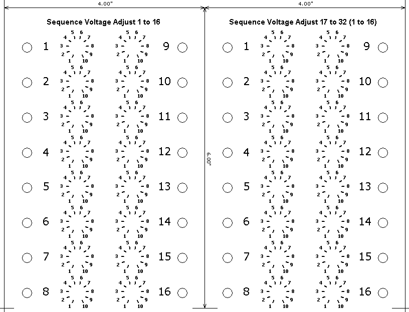
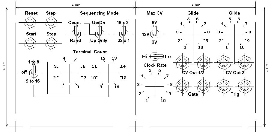
Front Panel Layout Ideas
32x1 and 16x2 Sequencer Project Parts List
| Qty. | Description | Value | Designators |
|---|---|---|---|
| 3 | CD40106 Hex Inverter(s) | CD40106 | IC2-F, IC2-C, IC2-A, IC2-B, IC2-D, IC2-E, IC6-A, IC6-B, IC6-C, IC6-C, IC6-D, IC6-E, IC13-A, IC13-B, IC13-C, IC13-E, IC13-F, IC13-D |
| 1 | CD4013 Dual D Flip Flop | CD4013 | IC7-A, IC7-B |
| 2 | CD40193 4-Bit Binary Ctr(s) | CD40193 | IC4, IC5 |
| 1 | CD4070 XOR Gate | CD4070 | IC10-B, IC10-A, IC10-D, IC10-C |
| 1 | CD4094 Shift Register | CD4094 | IC3 |
| 2 | CD4514 - 4 to 16 Line Decoder(s) | CD4514 | IC8, IC9 |
| 5 | Ceramic Capacitor(s) | .001uF | C4, C9, C10, C19, C15 |
| 3 | Ceramic Capacitor(s) | .005uF | C5, C6, C8 |
| 3 | Ceramic Capacitor | 0.1uF | C3 (Additional 2 for power supply bypass caps) |
| 1 | Ceramic Capacitor | 0.22uF | C2 |
| 3 | Ceramic Capacitor(s) | 1.0uF | C14, C11, C16 |
| 1 | Ceramic Capacitor | 100pF | C1 |
| 1 | Ceramic Capacitor | 1uF NP | C18 |
| 1 | DPDT Switch (Center Off) | DPDT | S8 |
| 1 | DPST Switch | DPST | S1 |
| 2 | Electrolytic Capacitor(s) | 10uF | Power supply bypass caps. |
| 1 | Electrolytic Capacitor | 15uF | C17 |
| 32 | LED(s) | LED | CR10(x16), CR11(x16) |
| 6 | Phone Jack(s) | 1/4" Jack | J3, J4, J1, J2, J5, J6 |
| 1 | Potentiometer | 1 Meg | R54 |
| 2 | Potentiometer(s) | 1M | R39, R32 |
| 32 | Potentiometer(s) | 50K | R24(x16), R28(x16) |
| 32 | Resistor 1/4 Watt 1%(s) | 100K | R27(x16), R23(x16) |
| 7 | Resistor 1/4 Watt 1%(s) | 10K | R5, R12, R3, R9, R13, R20, R21 |
| 2 | Resistor 1/4 Watt 1%(s) | 15K | R36, R44 |
| 8 | Resistor 1/4 Watt 1%(s) | 1K | R2, R6, R40, R45, R33, R37, R49, R53 |
| 3 | Resistor 1/4 Watt 1%(s) | 1M | R11, R8, R52 |
| 9 | Resistor 1/4 Watt 1%(s) | 200K | R14, R16, R15, R19, R18, R17, R56, R50, R51 |
| 1 | Resistor 1/4 Watt 1% | 20K | R55 |
| 1 | Resistor 1/4 Watt 1% | 2M | R1 |
| 1 | Resistor 1/4 Watt 1% | 30K | R57 |
| 3 | Resistor 1/4 Watt 1%(s) | 3K | R22, R26, R58 |
| 2 | Resistor 1/4 Watt 1%(s) | 4.7M | R7, R4 |
| 35 | Resistor 1/4 Watt 1%(s) | 470K | R29(x16), R25(x16), R30, R41, R48 |
| 8 | Resistor 1/4 Watt 1%(s) | 49.9K 1% | R34, R31, R38, R42, R43, R35, R46, R47 |
| 1 | Resistor 1/4 Watt 1% | 56K | R10 |
| 1 | SPDT Switch (center off) | SPDT | S5 |
| 1 | SPDT Switch | SPDT | S2 |
| 4 | SPST Push Button(s) | SPST | S4, S10, S9, S12 |
| 2 | SPST Switch(s) | SPST | S3, S11 |
| 2 | ST8T Rotary Switch (non-shorting) | SP8T | S7, S6 |
| 11 | Silicon Diode(s) | 1N914 | CR4, CR3, CR2, CR8, CR7, CR6, CR5, CR9, CR12, CR14, CR13 |
| 1 | Silicon Zener Diode | 1N4744 | CR1 |
| 1 | TLO82 Op Amp | TL082 | IC1-A, IC1-B |
| 2 | TLO84 Op Amp(s) | TL084 | IC11-A, IC11-B, IC11-C, IC11-D, IC12-A, IC12-B, IC12-C, IC12-D |
| 32 | Transistor NPN(s) | 2N3904 | Q1(x16), Q2(x16) |