Ray Wilson authored this content while he was actively running MFOS as the founder and resident genius.
We retain the content because it reflects a valuable point of view representing that time and place.
Article by Ray Wilson
Table of Contents...
- Introduction
- Schematic Page 1 Description
- Schematic Page 1
- Schematic Page 2 Description
- Schematic Page 2
- Schematic Page 3 Description
- Schematic Page 3
- Scope Photos
- A to D Timing Diagram
- Clock Quantizer Timing Diagram
- 16 Step Sequencer Quantized Vari-Clock Module PCB Information
- 16 Step Sequencer Quantized Vari-Clock Module Parts List
- Integrating the Quantized Clock Circuit Into the MFOS 16 Step Sequencer
- Wiring Diagram for Sequencer With Integrated Vari-Clock Circuit
- Suggested Panel Layout
- The Design Journey In Photos
Introduction
Table of Contents...I can't emphasize enough the value of reading over the whole project before getting started. It will greatly contribute to your project's success.
The phase shift oscillator comprised of U1-A (1/6 CD40106), R26 (20K) and C17 (680pF) needs to be oscillating at about 54KHz. Much of the logic in this circuit is based on fixed time intervals created by RC delays. If the clock is not at the correct frequency the circuit will not function properly. If necessary the clock frequency can be increased or decreased by adjusting the value of R26. Make R26's value higher to slow the rate or lower to increase the rate.
I started thinking about a simple way to allow me to change the duration of each step in a 16 step sequencer but do it in a quantized manner. This circuit accomplishes that goal elegantly and if you ask me fairly simply. You can build this as a stand alone (wired into your existing MFOS 16 Step Sequencer) but I suggest you add LED annunciators for each step so you can easily coordinate between the existing sequencer's pitches and this new module's durations. The same type of arrangement I suggest for adding LEDs to additional MFOS Sequencer analog boards will work for this project. See the bottom portion of the original MFOS 16 Step Sequencer project page for that information.
I believe the 1/16 note duration quanta are sufficient to provide some very interesting sequences. The sequencer's main clock adjustment affects the entire quantized sequence since the step durations are in main clock intervals. Two gate modes allows the sequencer to have a gate that goes high for 1/2 of each step's duration or multiple gates per step. The multiple gates occur at the main clock rate so that you can select from 1 to 16 gate pulses per step (a totally cool feature). For example this means that you can have a sequence that goes: E-E-E-E G-G-G-G D-D-D-D A-A-A B -> reset using only 5 steps of sequence. The first step would be set to emit 4 pulses, the second step would be set to emit 4 pulses, the third step would be set to emit 4 pulses, the fourth step would be set to emit 3 pulses, the fifth step would be set to emit 1 pulse, and then the sequencer would reset (if set to reset at terminal count). If you have selected reverse action at step then the sequencer would reverse instead of reset but each step will still have it's set number of pulses regardless of sequence direction.
Integration With MFOS 16 Step Sequencer
This circuit is designed to be used with the MFOS 16 Step Sequencer. Integrating this clocking scheme into the current MFOS 16 Step Sequencer is not hard and merely requires the removal of a few components on the sequencer's digital board and a few connections between the MFOS 16 Step Sequencer digital board and the new Quantized Vari-Clock module. After integration of this module with your new or existing MFOS 16 Step Sequencer, gate output is controlled by the gate control switches (as before) but there are some modifications to make to support a new gate mode. The modification requires one careful trace cut on the top of the PC board in a very accessible area. There are two plated-through vias (on the ends of the trace that gets cut) exactly where we need them for convenient wiring to the panel.
I will fully explain the new functionality of this module first and then I will add a section on integrating the module into your existing sequencer. I built an entirely new sequencer for this project (now I have two) and I plan to modify my existing sequencer to have this functionality. I will show the panel diagram for the new sequencer I built in case you want to build it the same way.
Schematic Page 1 Description
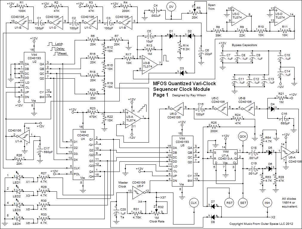
Table of Contents...In order to achieve quantized durations I started out by designing the mechanism by which a normal pot could be used as a digitized pot since I need each pot's setting to be converted to a number between 0 and 15. I use that information to determine the duration for each step. I accomplished this by designing an analog to digital convertor that could take a pot's position and convert it to a number between 0 and 15 relatively quickly (within 300 microseconds or so). The A to D convertor is the type that uses a D to A convertor to create a stepped ramp voltage to which the input is compared. When the stepped voltage output of the D to A convertor is a few millivolts above the current input level the current count from the D to A convertor is clocked into a latch. The latched output is the D (digital code) in this A to D convertor. The circuitry is described below.
The A to D convertor is realized by U1, U2, U3 and U4. U2 is a CD40193 binary counter whose outputs are connected to the classic R/2R network (made up of R6, R7, R12, R16, R15, R18, R19, R20 and R22) which converts the binary output to a voltage level which is linearly related to the binary count (I refer to this as the D to A element of the A to D convertor). R23 (470K to +12V) causes the output of the R/2R ladder to be positively biased a bit. This is to allow sensing of zero volts by the A to D convertor.
The counter is clocked by U1-A, C17 and R26 which are wired as a simple phase shift oscillator. The CD40193 is wired to count upward and thus the output of the R/2R ladder (D to A) is a positive going stepped ramp wave whose voltage levels correspond with the binary output of the counter. U3-A buffers the R/2R network output and applies it to the non-inverting input of U3-B via 10K resistor R17. U3-B's inverting input is connected to the level shifted input voltage (Point DV).
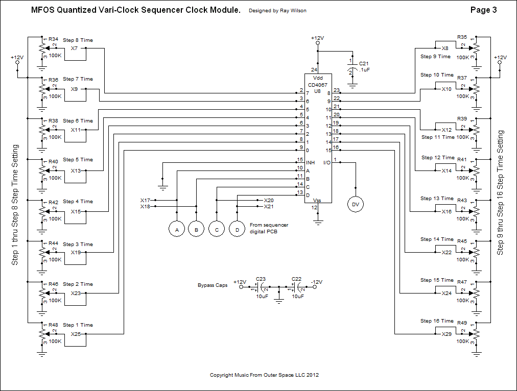
Point DV connects to the common I/O point on U8 CD4067 16 channel analog switch. The inputs to the CD4067 are the wipers of the pots used to set the step durations. The pots are wired as variable voltage dividers delivering between 0V and 12V to the wiper as the pot is advanced from CCW to CW. The CD4067 connects one of the pot wipers at a time to it's common I/O (pin 1) depending on the binary code applied to it's A thru D channel selection inputs. For example code 0000 connects pin 9 to the common I/O point pin 1.
As the CD4067 connects one of the pot wipers to the common I/O point the voltage on the wiper is applied to circuit point DV (duration voltage). The voltage is attenuated slightly by U3-C and resistors R8 and R9 wired as an inverting attenuator (gain of -.56). Trimmer R5 is used to trim the voltage to allow the full rotation of the pot to take the duration smoothly through the 16 settings. U3-D re-inverts and buffers the voltage so that it's output corresponds with the sense of the voltage applied to point DV.
Span Calibration
In order to utilize the full rotation of the duration pots for setting the digital code you need to adjust trimmer R5. Calibrating the span trim is easy. With the sequencer in step mode, step to any position. Turn that position's duration pot all the way up. Adjust R5 until all of the binary indicator LEDs (LED1 thru LED4) are lit. Now adjust the pot until the 1's place LED (LED1) goes out then adjust R5 so that the 1's place LED (LED1) just comes on and then turn it a wee bit further so that all the LEDs are solidly lit when the pot is adjusted fully clockwise. During use you will want to adjust the duration settings so that the binary count indicator LEDs are solidly on. You want to make sure you are at the sweet spots of the pot's adjustment and not at a quasi-in-between setting. With use of the feature this becomes second nature.
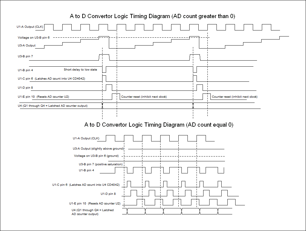
U3-D's output is applied to the inverting input of U3-B which is wired as a comparator. During normal operation the output of U3-A is compared to the voltage present at U3-D's output. When the voltage at U3-B pin 5 (output of the D to A) goes above the voltage present on U3-B pin 6 the output of U3-B rapidly shoots from low saturation (-11.5V) to positive saturation (+11.5V). The voltage on the output of U3-B forward biases D1 (all diodes are 1N914 or equivalent) causing U3-B's high level minus a diode drop to be dropped on R14 (6.2K resistor). Prior to U3-B going high D1 was reverse biased allowing C6 to discharge via D2 and R14 to ground keeping the output of U1-B at a high logic level. When U3-B's output is at positive saturation the voltage drop on R14 reverse biases D2 and allows C6 to charge via R4 to +12V in about 5uS. Thus at the moment U3-B's output goes high U1-B's output goes low after about 5 uS. U1-B's output returns high when the A to D clock goes low.
When U1-B's output goes low a chain reaction occurs through the Schmitt trigger inverters (U1-C, U1-D, and U1-E). As U1-B's output goes low it pulls current through C3 momentarily bringing U1-C pin 5 low and correspondingly U1-C's output pin 6 high for about 2uS. The side of C3 connected to the input of U1-C gets recharged by R3 very quickly and so the output of U1-C returns low after about 2uS. In the same manner U1-C going low causes a fast high going pulse on the output of U1-D which, when it returns low, causes yet another high going pulse to be emitted by U1-E. What we achieve here is a short pulse that occurs about 5uS after the R/2R ladder's (D to A) voltage crosses the level of the input voltage (output of U1-C applied to U4's CLK input), an approximate 5uS delay (output of U1-D), and then another approximate 10uS pulse that is used to zero the counter (output of U1-E applied to U2's CL-ear input) starting another sampling cycle. A tricky little bit to understand here is that the reset pulse overlaps the next clock cycle's rising edge and thus inhibits it from clocking the counter. That is very important because without the overlap the AD convertor is unable to sample 0 volts.
The count at the output of U2 at the moment the R/2R's output exceeds the duration voltage set by the pot and fed through U8 and level shifted by U3 is latched into CMOS Quad Clocked 'D' Latch U4. So as we connect one of the duration setting pot wipers to the A to D the digitized level on that pot is stored in U4 in less than 300uS. The latched count is displayed on LED1 thru LED4. As a sequence step's duration pot is adjusted these LEDs let you know the current setting for that particular duration pot. It is important to note that the duration is always the binary count displayed by the LEDs + 1. Thus 0000 corresponds to 1 master clock duration and 1111 corresponds to 16 master clock durations for any step.
D3 connects the input of U1-B to the clock which drives the A to D convertor. When the inverting input of U3-B is lower than the lowest level the D to A can output, which remember is a bit offset above ground via R23, the output of U3-B goes and stays at positive saturation. D3 allows the clock signal to continue to switch the input of U1-B high and low because when the clock goes low D3 is forward biased which discharges C6 and causes U1-B pin 4 to go high. When the clock goes back high again D3 is reversed biased and C6 is rapidly charged via R4 making the output of U1-B rapidly go low. This scheme allows the A to D to sample and latch the 0 level into U4.
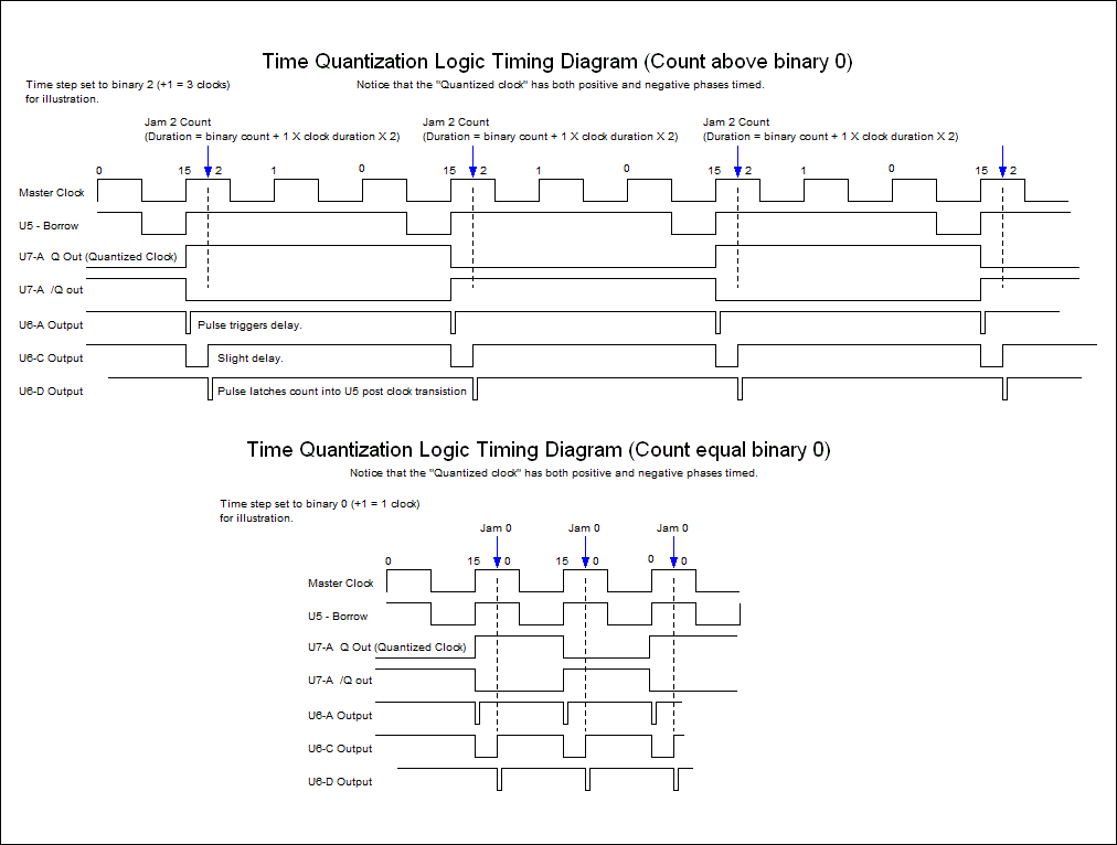
Well now we know how the A to D portion of the circuit works. Getting the duration right was a small challenge as well. In order to really control the duration of the clock both the high time and the low time of the clock must be quantized equally. We accomplish this by timing both the quantized clock's high time and it's low time.
The main clock is comprised of U6-F and associated components C20, R31 and 1M linear Clock Rate adjust pot R32. Note that U5 a CD40193 binary counter is clocked down by the positive edges of the main clock. The borrow output of the counter clocks one half of CD4013 Dual D Flip Flop U7 when the counter counts to zero. The flip flop is wired so that it takes two transistions of the borrow output to generate one full quantized clock cycle (which is the Q output of flip flop U7-A). This is how we time both the high and low phases of the quantized clock. When either output of the flip flop goes high a low going pulse is generated at the output of U6-A. This is because only the front edge of the Q or NOT-Q outputs is driven through C18 when the Q goes high or through C19 when the NOT-Q goes high. The front edge of either pulse is conducted through forward biased D5 (Q output goes high) or D6 (NOT-Q output goes high) and dropped on resistor R28. The low going pulse at the output of U6-A pulls current through D4 and discharges C16 to ground almost immediately causing U6-B's output to go high and U6-C's output to go low. By this time the output of U6-A has returned high again reverse biasing D4 and allowing C16 to charge through R21 to +12V. Thus U6-B's output goes low and U6-C's output goes high. U6-C's low to high transition pushes a pulse through C15 which results in a short low going pulse at the output of U6-D which causes CD40193 counter U5 to load the latched count presented to it's data inputs by CD4042 quad latch U4's Q outputs. The sequence is advanced to the next step when the Q output of U7-A goes low (I know that seems a little counter-intuitive but that's what the point where the clock is injected into the sequencer board expects).
For example let us imagine that U7-A's Q output has just gone low. We have stepped to the next sequence step and the duration voltage for the step is applied to the input of the A to D convertor. We will consider what happens if the duration pot is currently adjusted to cause the number 2 (0010) to be latched into the A to D's binary latch.
Main clock begins to clock U4 down. When U4's count reaches 0 because the main clock's positive edge just clocked it to 0 the borrow output of U5 goes low concurrent with the main clock's next low phase (see chart). Counter U5 wraps to 15 on the clock's next rising edge but during the high portion of that clock and prior to the next low to high clock edge we jam the 2 count into counter U5 again so that the next edge clocks down to 1, next 0, next 15 but we immediately jam the 2 count into counter U5 again and the cycle continues. The wrapping to 15 and subsequent jamming of the duration count into the counter is what allows us to jam counts from 0 to 15 into the counter resulting in durations that range from 1 clock (LEDs indicate binary 0) to 16 clocks (LEDs indicate binary 15). So the thing to remember is that when you are observing the LEDs used to display the current step's duration you need to take the binary number represented by the LEDs and add 1. Thus a display of 0000 (all binary count display LEDs off) indicates that the step's duration is 1 time quanta long and a display of 1111 (all binary count display LEDs on) indicates that the step's duration is 16 time quanta long. In a way you can think of this as adjusting the step's duration from 1/16 note to a whole note in increments of 1/16 note.
To repeat, when the A to D latches 0 (0000) we still count 1 step each time 0 is latched into the counter's presets. (see chart).
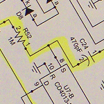
We mentioned above that we need to time both the high phase and the low phase of the quantized clock in order for this scheme to work. Thus, for example, if we have selected a duration of 8 quanta for a step (binary count display shows... have you been reading...? 0111 - CORRECT!) the main clock makes 8 low to high transitions during the high phase and 8 low to high transitions during the low phase. In order to generate the number of pulses that correspond to the selected duration we divide the main clock's frequency in two. The other half of U7-B (CD4013 Dual D Flip Flop) is used to divide the master clock's rate in half. Now the Q output of U7-B will make the number of transistions that corresponds to each step's duration setting. In order to insure that U7-B's Q output is synced so that it goes high at the proper time we use the NOT-Q output of U7-A (remember that Q going low advances the sequence so NOT-Q goes high as the sequence is advanced) to kick U7-B into the proper state and then the normal divide by two action does the rest. The "kick" comes through C24 (470pF cap) and is dropped on R52 (1M resistor) the binary divide by two operation of the D Flip Flop wired so that the NOT-Q is fed to the D (data) input does the rest. Without synchronization the output of U7-B would be correct... but only half of the time.
The big question... WHY RAY? Good question. This scheme's raison d'etre is to provide two gate modes for the sequencer. In mode one (Normal) the gate output is high for one half of the step's selected duration. In mode two (Multi) the sequencer emits the number of gates that correspond to the step's duration count and they are emitted at the main clock's rate divided by two. So... if you have a step set to 8 (binary display 0111) the sequencer will output 8 gates during that step.
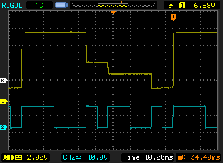
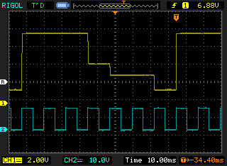
Scope Photos Showing Gate Modes (Reset at count 5, Yellow = step voltages, Blue = gate output.)
Sequencer rate at maximum in order to fit enough steps into the scope photo to capture the idea.
| Normal Mode. The gate output goes high for half of the step's duration. Here we see: step 1 set to a duration of 3 (binary count displays 0010), step 2 set to a duration of 1 (binary count displays 0000), step 3 set to a duration of 2 (binary count displays 0001), step 4 set to a duration of 1 (binary count displays 0000). | Multi Mode. The gate output goes high and low the number of times that corresponds to the step's duration setting. Here we see the effect of Multi gate mode with the same setup. Note that the gate train always starts high as the step changes as you would expect. |
 |
 |
It is important for the sequencer's gate control switches to control the output of a channel whether the sequencer is in multi-gate or normal mode. To do this we use S3 to select whether the MFOS 16 Step Sequencer's UP/DN clock or the Q output of U7-B is used to diode AND with the outputs of the CD4514 to result in a gate output. Remember that the outputs of the CD4514 go high one after the other with no break in between. If we just used that for the gate output the gate would never go low so we AND either of these digital clock sources with the CD4514 outputs so that they go low at the appropriate time and the gate output works properly.
Schematic Page 1
View as PDF Table of Contents...
Schematic Page 2 Description
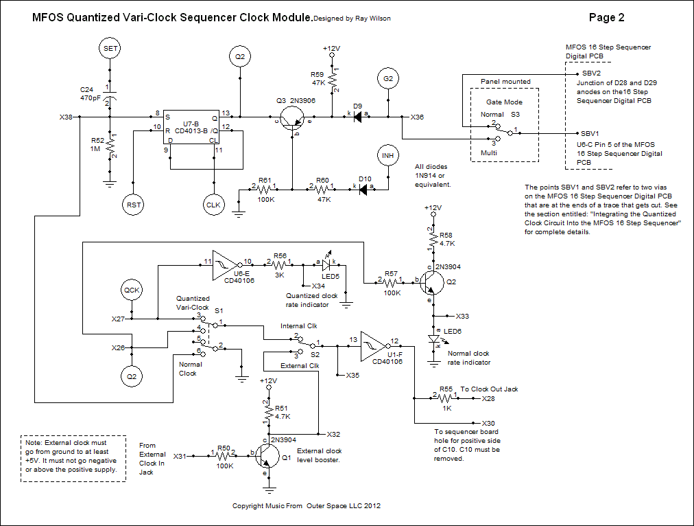
Table of Contents...Here we see the other half of U7 dual D flip flop (U7-B) which is used to divide the main clock's frequency in half. The Q output is used for the multi-gate functionality. The job of 2N3906 PNP transistor Q3 is to keep the low state of the Q from inhibiting the gate output when we are in step mode. When we stop the sequencer by pressing the Stop/Run button to put the sequencer into the stopped state point INH goes high. When point INH is high diode D10 is forward biased and the base of PNP transistor Q3 sees the positive voltage dropped on R61 which turns Q3 off and keeps U7-B's low Q output from forward biasing D9. Circuit point Q2 on the other hand needs to go low when the clock inhibit (point INH) is high. When the sequencer is in the running state circuit point INH goes low reverse biasing diode D10. R61 100K resistor holds the base of Q3 low and turns it on allowing D9 to bring point X36 low whenever the Q output is in the low state. Diode D10 isolates the output of U7-B's Q output which forward biases the C-B junction of Q3 when it is high.
Point X38 goes to switch S1 which grounds the junction of C24, R52 and pin 8 of U7-B when in Normal clock mode. This is so the pulses coming through C24 (which normally are used to insure that U7-B is properly synced in Vari-Clock mode) do not inappropriately set U7-B and interfere with the Normal clocking mode.
The clock selection circuitry uses CD40106 inverters and transistors to get all of the various clocks and LED displays to "jive" (a very technical term) with what the MFOS 16 Step Sequencer requires. The external clock input is boosted by Q1 (external clock level can be as low as 5V) and inverted prior to being fed to the input of inverter U1-F. Circuit point QCK (Q output of U7-A) signal is inverted prior to the LED display and Q2 merely buffers the Q output of U7-B to light the LED which indicates the sequencer's normal rate. The output labeled X30 is fed to the MFOS 16 Step Sequencer and replaces the clock source of the original.
Note: In Quantized Vari-Clock mode, both gate modes can be used (Normal and Multi). In Normal clock mode only Normal gate mode should be selected. When Multi gate mode is selected in Normal clock mode the gate output is not synchronized with the voltage changes but instead occurs half way through each voltage step's time. I did not correct this since the unit works fine in Normal gate mode with Normal clock mode. Multi gate mode would not make any difference under these conditions and someone may find the anomaly useful for some effect.
Schematic Page 2
View as PDF Table of Contents...
Schematic Page 3 Description
Table of Contents...Schematic page 3 shows the CD4067 used to steer each sequence step's duration setting voltage to the circuitry that converts it to the step time. Each pot's wiper delivers from 0 to +12V which is steered via U8 to the remaining circuitry. The channel selection inputs (A thru D) are connected to the output of the MFOS 16 Step Sequencer's main counter chip (U4 of the MFOS 16 Step Sequencer). All interconnections between this PC board and the MFOS 16 Step Sequencer are explained in the section entitled "Integrating the Quantized Clock Circuit Into the MFOS 16 Step Sequencer".
Schematic Page 3
View as PDF Table of Contents...
Scope Photos
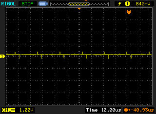
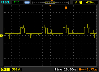
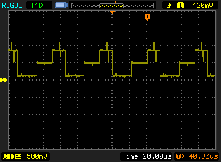
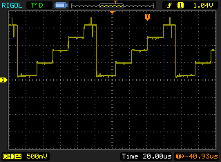
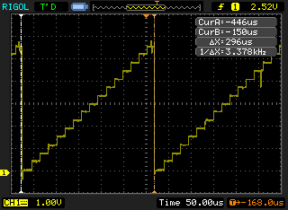
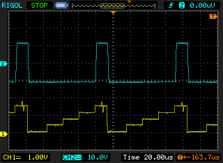
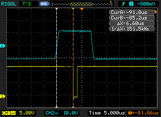
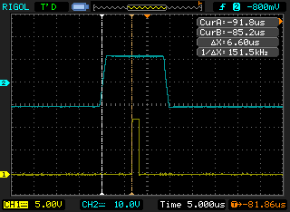
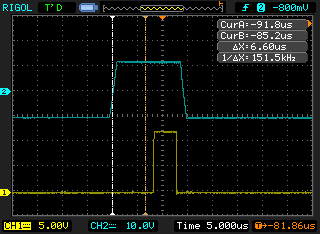
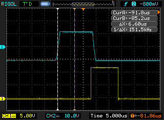
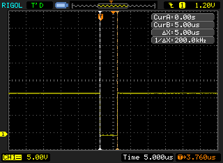
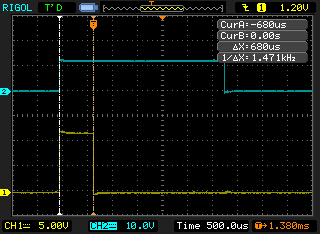
Table of Contents...If you run into trouble shooting issues these scope photos may help you track down the problem. Use the cues from the photos (time scale, voltage scale, cursor positions, etc) to determine what each photo represents in the voltage and time domains.
| Observing U1-A pin 2. This is the A to D clock signal. It must be approximately 54 KHz give or take a KHz. | Observing U3-B pin 7 with sequencer in stopped mode, step one selected, and step 1 duration set to 2 (only LED 1 on). Note that when step time is set to 0 U3-B pin 7 is always at positive saturation (approx 11.5V) | Same as previous except step 1 duration set to 8 (LEDs 1,2, and 4 on) |
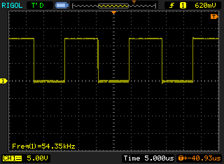 |
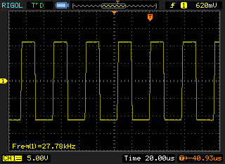 |
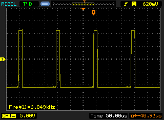 |
| Same as previous except step 1 duration set to 16 (LEDs 1,2,4 and 8 on) | Observing U3-A pin 1, step one duration set to 1 (no LEDs on) | Same as previous except step 1 duration set to 2 (LED 1 on) |
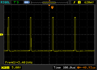 |
 |
 |
| Same as previous except step 1 duration set to 3 (LED 2 on) | Same as previous except step 1 duration set to 5 (LED 4 on) | Same as previous except step 1 duration set to 16 (All LEDs on) |
 |
 |
 |
| Observing U3-A pin 1 (Yellow) and U3-B pin 7 (Blue) step 1 duration set to 5 (LED 4 on) | Observing U1-B pin 4 (Yellow) and U3-B pin 7 (Blue) step 1 duration set to 5 (LED 4 on) | Observing U1-C pin 6 (Yellow) and U3-B pin 7 (Blue) step 1 duration set to 5 (LED 4 on) |
 |
 |
 |
| Observing U1-D pin 8 (Yellow) and U3-B pin 7 (Blue) step 1 duration set to 5 (LED 4 on) | Observing U1-E pin 10 (Yellow) and U3-B pin 7 (Blue) step 1 duration set to 5 (LED 4 on) | Observing U5 Load pulse pin 11 step 1 duration set to 5 (LED 4 on) |
 |
 |
 |
| Observing U6-B pin 4 (Yellow) and U5 pin 13 (Blue) step 1 duration set to 5 (LED 4 on) | ||
 |
A to D Timing Diagram
View as PDF Table of Contents...
Clock Quantizer Timing Diagram
View as PDF Table of Contents...
16 Step Sequencer PCB Information
Table of Contents...Changes in progress... I will repost after everything is solid on the board.
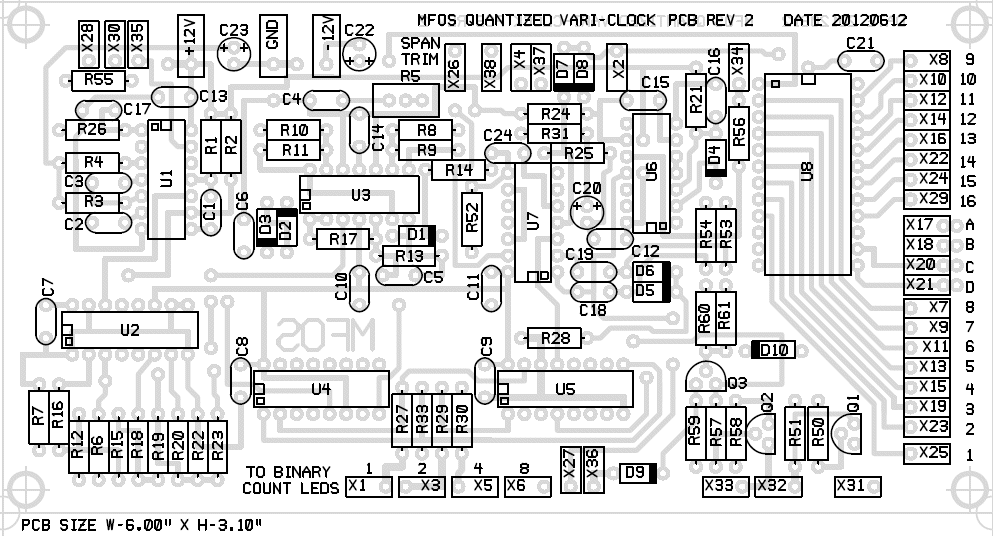
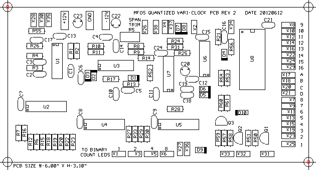
16 Step Sequencer Quantized Vari-Clock Module PCB Designators
View as PDF Table of Contents...Use this view during board troubleshooting where you will need to associate legend names with schematic values and component interconnections. There is a value view below so don't break your neck going between the schematic and the PCB during assembly.
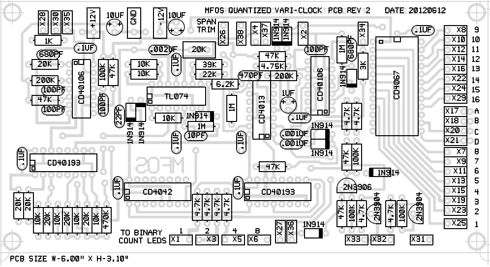
16 Step Sequencer Quantized Vari-Clock Module PCB Values
View as PDFUse this view during board population so you don't have to keep referring to the schematic to see what value relates to each designator. Just stuff the board with these values and voila... you're good to go.
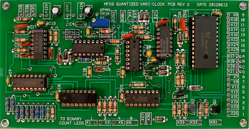
16 Step Sequencer Quantized Vari-Clock Module PCB Populated
You do not have to use the exact same style of parts as you see in this photo as long as they are the correct value and fit on the board (even with some lead forming).
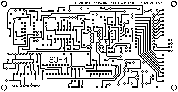
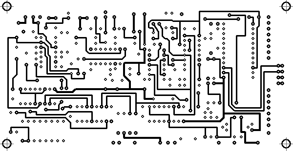
16 Step Sequencer Quantized Vari-Clock Module PCB Layouts
Bottom Copper
If you use these experiment with your drawing programs scaling until the ic pad centers are 0.1" apart and 0.3" across for the 8 or 14 pin DIP packages (all scaling will be correct once that is achieved).
Top Copper
Legend Silk Screen
16 Step Sequencer Quantized Vari-Clock Module Parts List
Table of Contents...
This list ONLY covers the Vari Clock module. Refer to the MFOS 16 Step Sequencer project for the parts required to construct the project anew (including the remainder of the MFOS 16 Step Sequencer).
All integrated circuits need to be DIP packages. When shopping for chips remember that the numbers will have suffixes like BE or BC but as long as they are DIP packages you will be fine. The suffixes typically indicate temperature ranges and package materials (plastic, ceramic, etc).
Using a 5% resistor for R31 will work. Using a metal film 1% resistor will give the clock oscillator more temperature stability.
Using 1% resistors in the A to D convertor is, I believe, imperative for best linearity of duration adjustment.
| Qty. | Description | Value | Designators |
|---|---|---|---|
| 2 | CD40106 | CD40106 | U1, U6 |
| 1 | CD4013 Dual D Flip Flop | CD4013 | U7 |
| 2 | CD40193 Presetable Four Bit Up Down Counter | CD40193 | U2, U5 |
| 1 | CD4042 Quad Clocked D Latch | CD4042 | U4 |
| 1 | CD4067 Analog Mux/DeMux | CD4067 | U8 |
| 1 | TL074 Quad Op Amp | TL074 | U3 |
| 2 | Transistor NPN 2N3904 | 2N3904 | Q1, Q2 |
| 1 | Transistor PNP 2N3906 | 2N3906 | Q3 |
| 10 | 1N914 High Speed Switching Diode | 1N914 | D1, D2, D3, D4, D5, D6, D7, D8, D9, D10 |
| 6 | General Purpose LED | LED | LED1, LED2, LED3, LED4, LED5, LED6 |
| 16 | Linear Taper Potentiometer | 100K | R34, R35, R36, R37, R38, R39, R40, R41, R42, R43, R44, R45, R46, R47, R48, R49 |
| 1 | Linear Taper Potentiometer | 1M | R32 |
| 1 | Multi turn trimmer (top adjust) | 20K | R5 |
| 1 | Resistor 1/4W 1% | 4.75K | R31 |
| 4 | Resistor 1/4W 1% | 10K | R12, R15, R19, R22 |
| 5 | Resistor 1/4W 1% | 20K | R6, R7, R16, R18, R20 |
| 4 | Resistor 1/4W 5% | 100K | R1, R50, R57, R61 |
| 3 | Resistor 1/4W 5% | 10K | R10, R11, R17 |
| 1 | Resistor 1/4W 5% | 1K | R55 |
| 3 | Resistor 1/4W 5% | 1M | R13, R21, R52 |
| 2 | Resistor 1/4W 5% | 200K | R4, R25 |
| 1 | Resistor 1/4W 5% | 20K | R26 |
| 1 | Resistor 1/4W 5% | 22K | R9 |
| 1 | Resistor 1/4W 5% | 39K | R8 |
| 1 | Resistor 1/4W 5% | 3K | R56 |
| 8 | Resistor 1/4W 5% | 4.7K | R27, R29, R30, R33, R51, R53, R54, R58 |
| 1 | Resistor 1/4W 5% | 470K | R23 |
| 6 | Resistor 1/4W 5% | 47K | R2, R3, R24, R28, R59, R60 |
| 1 | Resistor 1/4W 5% | 6.2K | R14 |
| 2 | Capacitor Ceramic | .001uF | C18, C19 |
| 1 | Capacitor Ceramic | .002uF | C4 |
| 9 | Capacitor Ceramic | .1uF | C7, C8, C9, C10, C11, C12, C13, C14, C21 |
| 4 | Capacitor Ceramic | 100pF | C1, C2, C3, C15 |
| 1 | Capacitor Ceramic | 10pF | C5 |
| 1 | Capacitor Ceramic | 22pF | C6 |
| 1 | Capacitor Ceramic | 470pF | C24 |
| 2 | Capacitor Ceramic | 680pF | C16, C17 |
| 2 | Capacitor Electrolytic | 10uF | C22, C23 |
| 1 | Tantalum Capacitor | 1uF | C20 |
| 1 | Switch DPDT | DPDT | S1 |
| 2 | Switch SPDT | SPDT | S2, S3 |
| 17 | Knobs for pots |
Integrating the Quantized Clock Circuit Into the MFOS 16 Step Sequencer
Table of Contents...
|
OK, now that you know pretty much all about how this circuit works.
Now it's time to see how to integrate it into an existing (or newly built) MFOS 16 Step Sequencer.
It's pretty starightforward as you'll see. I suggest you refer to the information in the
original MFOS 16 Step Sequencer project
as you go.
Here is a photo of the prototype I built for this project. I plan to integrate one of these vari clock modules into my other sequencer because I really think it adds a ton of functionality and flexibility to the original. I used the same process for making this panel as I show on this page: How To Make Synth Panels. I show the panel layout and complete interconnections for this design below. By studying the diagram you will be able to identify where in your existing sequencer you need to make the interconnections. I believe it's pretty straightforward but if you find that the information is missing something vital please let me know so I can add clarifications. |
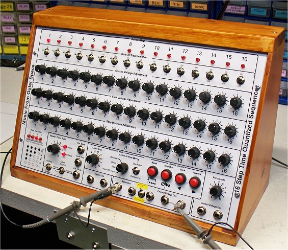
|
Remove (Or Don't Install) Original MFOS 16 Step Sequencer Clock Support Components
Several components associated with the original circuit's clocking function must be removed (or not inserted if building from scratch) from the MFOS 16 Step Sequencer Digital Board. Be careful when removing components to do so gently. My preferred method is to cut the leads close to the component and then grasp the remaining lead with a tweezer while applying the soldering iron. I use a nice sharp aluminum or stainless steel tweezers with small tips. Small tweezer tips suck up less heat. Make sure the solder is molten before applying gentle force to extract the lead otherwise you could damage the board. Use solder wick to remove the remaining solder. Don't use too much heat adjust your iron to around 350 to 400 fahrenheit range. Be careful with those solder suckers because they can become pad and trace suckers if you apply too much heat and delaminate the copper.
Components To Remove
- R18 (20K resistor)
- R23 (6.2K resistor)
- C10 (1uF capacitor)
- D9 (1N914 Diode)
- R43 (3.9K resistor)
- R41 (1K resistor)
- R24 (3K resistor)
- R42 (1K resistor)
- LED1 is no longer used.
- R19 (1M Clock Rate Adjust pot) is no longer used.
Location of components which must be removed from (or not installed on) the MFOS 16 Step Sequencer Digital Board
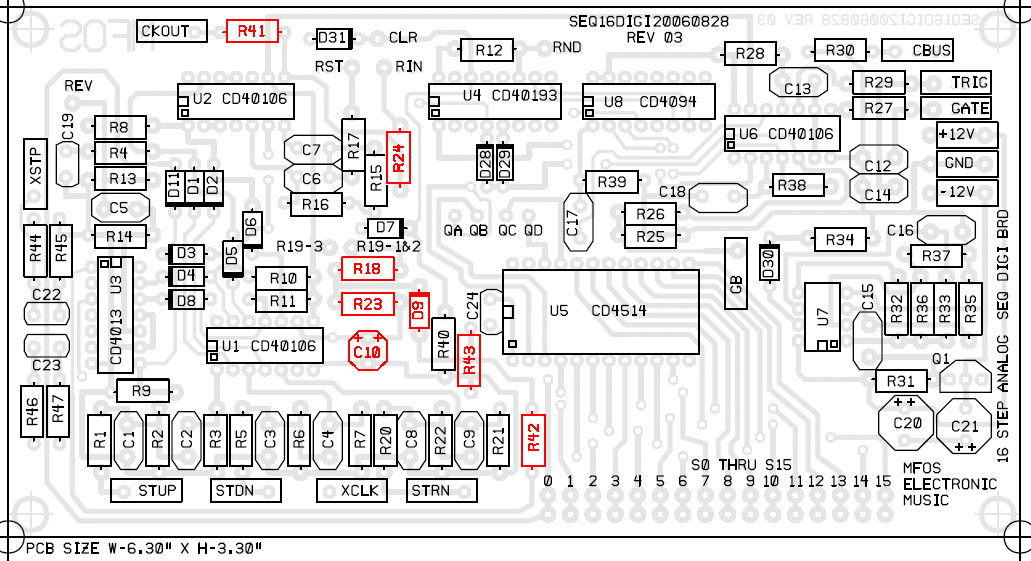
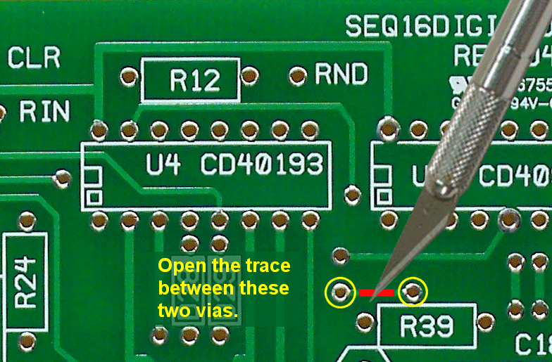
Trace Cut Between Vias on the MFOS 16 Step Sequencer Digital Control PCB
There is one trace cut on the MFOS 16 Step Sequencer Digital PCB that must be made. It is the trace near R39 (10K resistor) with two vias on the ends. The vias will be used to connect to the new board and panel in the modified sequencer so be careful not to damage them when you are cutting the trace. Use an exacto (or equivalent hobby knife) and be careful not to slip while cutting the trace and cut another trace you don't want or need to cut. It's easier than you think so be careful.
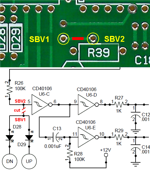
Plated Thru Via Designators and Schematic Relationship
|
In order to be able to refer to these two vias I am giving them names which I will use in explanations and
diagrams from now on. The MFOS 16 Step Sequencer schematic of what this trace cut and vias represent is also shown.
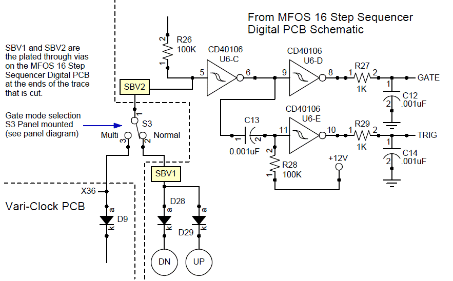
SBV1 connects to the anodes of D28 and D29 which are used as AND functions with the UP and DN clocks in conjunction with the digital outputs of the MFOS 16 Step Sequencer's Digital Board's U5 (CD4515BC 4-Bit Latched/4-to-16 Line Decoder). These diodes are part of the circuit which permits the gate to be controlled via the gate control switches of the sequencer. Part of the integration of the vari-clock board is to allow the gates generated by the new board to be controlled by the gate switches as well. |
|
Integration of Gate Control
The panel wiring diagram refers to the two points SBV1 and SBV2. Here is the schematic of how these points are integrated into the MFOS 16 Step Sequencer's Digital PCB. In the original MFOS 16 Step Sequencer's Digital control circuit the input of U6-C (don't confuse this with the Vari Clock Board's U6-C) is only allowed to see a high logic level through R26 if both the UP and DN clocks are high. If either is low the input of U6-C is held low (bringing the gate low). We use the same technique to allow the Vari Clock board to also control when the gate can be high via the Vari Clock circuit's point X36 which is connected in a similar fashion to the Vari Clock circuit's D9.
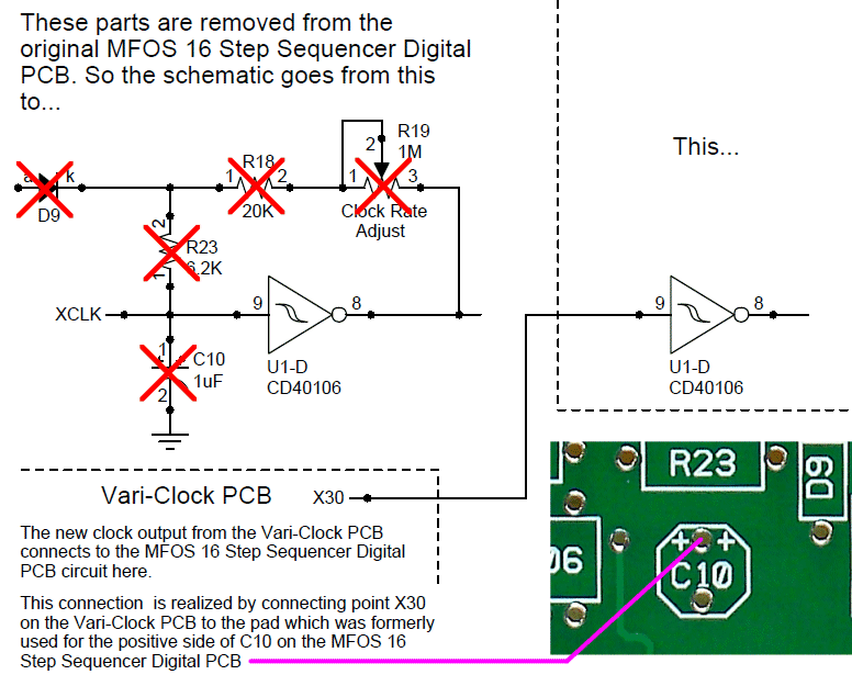
Integration of New Clock Source
The Vari-Clock circuit's clock output must be connected to the pad formerly used for the positive side of the MFOS 16 Step Sequencer's Digital control circuit's C10 (1uF cap). So point X30 of the Vari Clock board gets connected to the point shown. Components that must be removed from the MFOS 16 Step Sequencer's Digital control PCB are each shown with a red X.
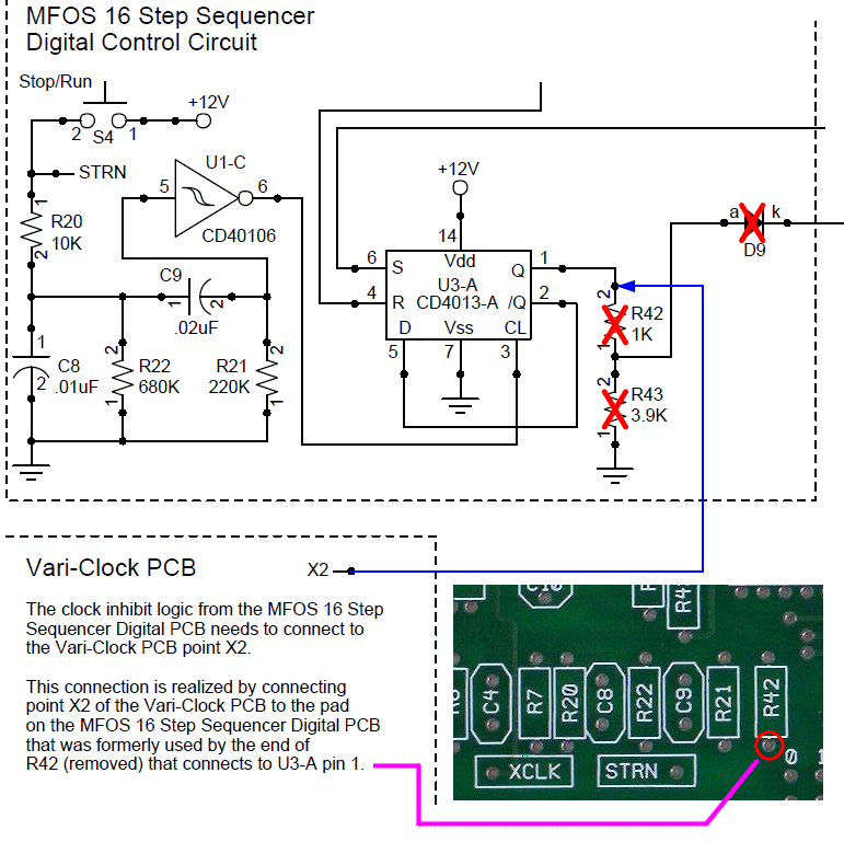
Integration of MFOS 16 Step Sequencer Clock Inhibit to Vari-Clock Circuit
The Vari-Clock circuit's clock needs to stop or run when the MFOS 16 Step Sequencer's Stop/Run button is pushed toggling the MFOS 16 Step Sequencer into either the stopped or running state. In order to accomplish this a connection must be made from the Vari-Clock circuit board's point X2 to the pad on the MFOS 16 Step Sequencer's Digital control PCB formerly used by the lead of R42 that connects directly to U3-A (CD4013-A) pin 1. R42 is one of the components that must be removed from the MFOS 16 Step Sequencer's Digital PCB when integrating the Vari-Clock module.
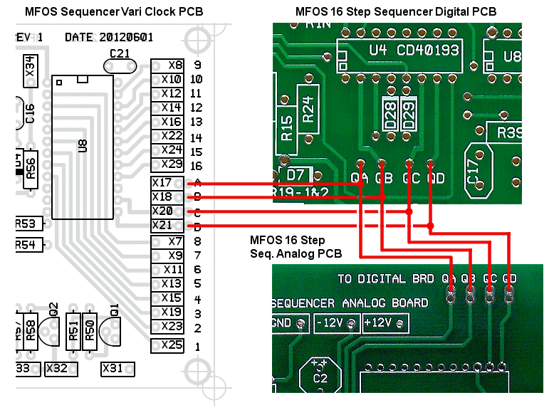
Integration of MFOS 16 Step Sequencer Clock Channel Select Lines
The Vari-Clock circuit's CD4067 chip needs to have it's A thru D channel selection lines connected to the MFOS 16 Step Sequencer PCB's A thru D channel selection lines. You can see from this diagram that the MFOS 16 Step Sequencer PCB's A thru D channel selection lines are connected in parallel to all three of the corresponding A thru D data selection lines of the three PCBs in this project. The Vari Clock PCB has two sets of pads for these lines. As long as all three of the PC boards have the data lines correctly connected in parallel it does not matter how the connections are daisy chained.
Wiring Diagram for Sequencer With Integrated Vari-Clock Circuit
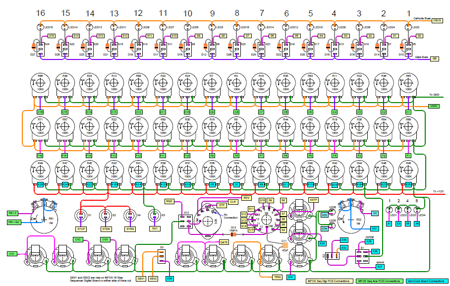
View as PDF Table of Contents...The remainder of the integration is best shown via this wiring diagram in which you see all of the interconnections between the panel and the PC boards. Much of this wiring is taken directly from the original MFOS 16 Step Sequencer project. I think this is clear enough to help people who are planning to modify their existing sequencer or who plan to construct an entirely new one. I suggest that you print out the documentation (schematics and panel diagrams) from the MFOS 16 Step Sequencer project as references while you build this whether you are modifying or building anew.
Here is the complete wiring diagram for a sequencer with the new Vari-Clock functionality wired in. By studying this diagram you can see how you would modify an existing sequencer or build an entirely new unit. You don't need to get out your magnifying glass just click the image to get a huge one or view it as a scalable PDF.
Notice the key that identifies which board connections go to. Blue colored connection indicators are for connections to the new Vari-Clock Module PCB, yellow colored connection indicators are for connections to the MFOS 16 Step Sequencer Digital control PCB and lastly green colored connection indicators are for connections to the MFOS 16 Step Sequencer Analog PCB.
Often browsers will apply scaling to fit the image to the viewport. Usually you can click it to zoom to actual size. What I do with large diagrams like this is use a graphics program (Gimp, Windows Paint, Paint Shop Pro, etc.) to cut the image up into pieces that fit on 8 1/2" x 11" paper (or whatever your normal page size is) and then tape it all together so I can have a nice large diagram to work from.
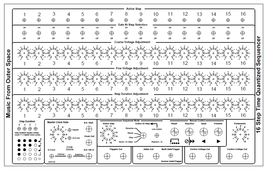
Panel Template for Sequencer With Integrated Vari-Clock Circuit
View as PDF Table of Contents...Click the PDF link above to open a one to one size PDF version of the panel template in Adobe reader. I made this panel the same way I always do by printing, laminating and then gluing the resultant applique to the panel. See: How To Make Synth Panels. In this case since I don't have a printer or plotter that prints that large I pieced the template together from 8 1/2" x 11" pieces of paper. My laminator is large enough for this but unfortunately my laminating sleeves weren't so I had to rely on laminate laminating to laminate (which worked fine) since it took a couple of laminating sleeves arranged to hold the pieced together paper template. I also had to make a paper sleeve to hold the paper and laminate before feeding the whole thing into the laminator since the one that came with the laminator was not large enough. It's never a good idea to expose laminate directly to the hot rollers in the laminator (it has a penchant to curl).
The template is designed for a 16" x 10" piece of front panel material. I used 1/16" thick aluminum plate from METAL supermarkets.
Unfortunately I have no real concrete advice on printing this out since it is so large. You could go to an office supply store that has a print center (which many do) and bring the PDF with you and have it printed on a large format printer or plotter. The alternative is to do it the hard way and play with copying and scaling with your graphics program until you can print out the image piece-meal and tape or glue the individual pieces together neatly.
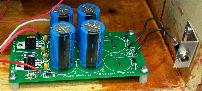
Power Provided By MFOS Wall Wart Power Supply Circuit
I used an MFOS Wall Wart supply for this project and as you can see I only added four of the six possible main filter caps since the whole sequencer circuit (including Vari Clock) only draws about 40 to 50 milliamps from each side of the +/-12V supply. I did not need to use heat sinks and the regulators hardly get warm. I always isolate the secondary connection of the wall wart from the remaining circuit to eliminate the possibility of shorting the output due to jack wiring.
The Design Journey In Photos
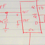
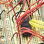
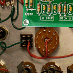
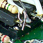
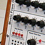
Table of Contents...Here are some photos from the design process for this project. It was kind of challenging to get the functionality I wanted without a bunch of digital pots and a microprocessor etc. I think this project came out nicely. From concept to completion took a couple of months because I had a few other things going on. Once I verified the design during the breadboard stage I had a prototype board ordered. As you can see the prototype version 0 got kind of kludgy when I rethought a couple of things. I ordered a second prototype and learned a valuable lesson... NEVER order prototypes until ALL of the bugs and enhancements for the previous prototype are COMPLETELY ironed out or when your second prototype comes you'll have to put it on a shelf and forget about it (anyone need some soldering practice boards...). I ordered a third prototype board to make sure the revised design was solid and that I hadn't forgotten anything. The third board was a charm and everything worked as expected. It's a fair amount of work to come up with these designs but I love every minute of it. I hope you enjoy this project and that it helps you with your creative endeavors. Peace.
 |
 |
 |
 |
 |
|
 |
 |
 |
 |
 |
|
 |
 |
 |
 |
 |
Now it's on to the next project...
