Ray Wilson authored this content while he was actively running MFOS as the founder and resident genius.
We retain the content because it reflects a valuable point of view representing that time and place.
Article by Ray Wilson
PC Board Part Designators
View as PDF ...OR... View as Large ImageThis view is good when troubleshooting so you can go from the schematic to the PC mounted component by designator.

PC Board Part Values
View as PDF ...OR... View as Large ImageThis view is good when populating the board so you don't have to go back and forth between the board and the schematic looking for each designator.

PC Board Populated
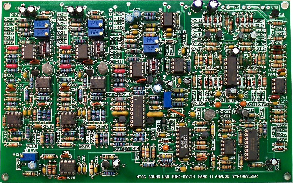
View Larger ImageHere is a picture of the populated PC board. I had to kludge R118 in since this was a prototype PCB and I changed the bias of the Sample & Hold from two resistors to the trimmer for more accuracy. This was the second prototype PCB. I had to relayout the noise section because in the first prototype the component layout contributed to odd capacitive feedback between the components in the high gain noise section. So after making the first prototype and then this one I can live with one kludge but the production boards are laid out for the R118 100K trimmer so you don't have to. You may note that I used 0.1% precision resistors for some of the control voltage summing resistors in the VCOs and VCF. I did this so they would both respond more consistently to keyboard control voltage (this is not required).
When populating the board I work from lower to higher profile components: resistors, sockets, capacitors, transistors, etc. I also solder the components from the top of the PC board (this is a preference, not required in any way). This way I can populate a number of components on the board while it's in my Panavise and then solder them. I continue to do this and then when I have all of a particular value or type I turn the board over and trim the leads. If you do it this way you need to use a lead trimmer that applies very low to no shock to the soldered joint. Some people prefer to trim the leads and then solder to avoid mechanically shocking the solder joints at all but I have had good success with my technique. The plated through holes make top and bottom fillets no matter whether you solder from the top or from the bottom. I check over the look of the bottom joints and if I see one that needs a touch up I just reheat it and add a small amount of solder or desolder it completely and redo it if necessary.

Module Map
Here is a quck overview of the board for when you need to troubleshoot. You can look in the correct area without having to find it again every time you need to.

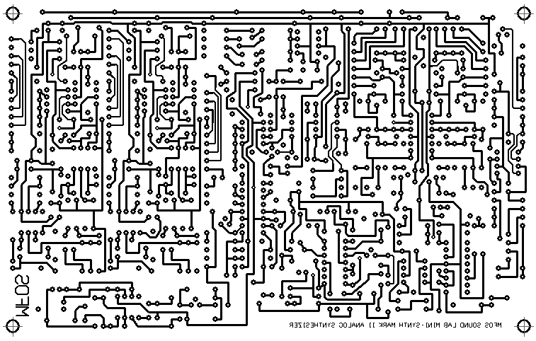
PC Board Bottom Traces For Reference or Home Fabrication
Before I began to order prototype boards I used to use these same type layouts to fabricate my boards using a photo sensitive resist PCB process.

PC Board Top Traces For Reference or Home Fabrication

PC Board Silkscreen For Reference or Home Fabrication
