Article by Ray Wilson
Introduction
This would be a perfect circuit for the Sound Lab because it is simple and relatively low current. After I breadboarded this I sat and played with it for about an hour because it was non-stop fun. The varying patterns and effects had me mesmerized.
Circuit Description
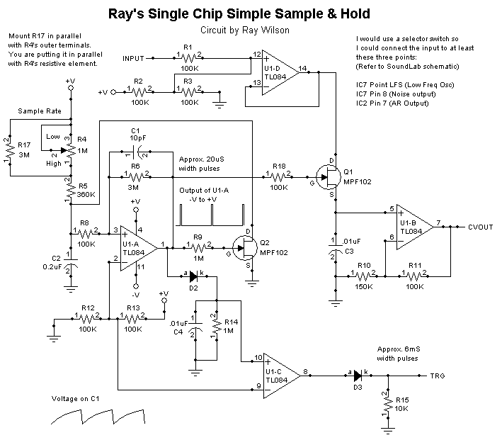
Here is how it works. In order to sample and hold we need a sample clock. The sample clock is comprised of U1-A and associated components (R4, R5, C2, R8, C1, R6, R12, R13, R9 and Q2). Current flows through R4 and R5 and charges C2. The voltage on C2 is presented to U1-A's non-inverting input via R8. When the voltage rises above 1/2 +V it causes U1-A's output to go high and turn on Q2 which quickly discharges C2 enough to cause U1-A's output to go low again. This results in a 20uS pulse on the output of U1-A. The pulse's high time is the time it takes C2 to discharge through Q2 (drain to source) to the level which causes U1-A to go low again. At higher voltage power supplies (+/-12V or +/-15V) the oscillator may stop at the extreme end of R4's adjustment range. You can tweak the value of the resistor in parallel with R4 (make R17 a bit lower in value) or R5 (also a bit lower in value BUT NEVER LOWER THAN 10K) to prevent that. This cycle repeats resulting in the sample clock. The sample frequency is adjusted with R4 Sample Rate pot. R6 provides a bit of hysteresis for the comparator and C1 squares up the pulse edges with a shot of positive feedback. The pulse that results at the output of U1-A is about 20uS wide and goes from -V to +V which is what we need to control the gate of the sample FET Q1.We connect the gate of the sample FET to the pulses via R18. When U1-A's output is low the FET is turned off (S and D do no conduct) but when a pulse occurs Q2's gate is brought high which essentially shorts S and D and allows the voltage on Q1's drain to charge (or discharge) C3 to the voltage at U1-D's output. U1-B is a high impedance buffer with a bit of gain added by R10 and R11. It provides the output buffering for the sampled and held voltage on C3. C3 will droop slowly but not enough to hear with samples occurring at or above 1 per second or so.
U1-D is the input buffer and is biased to 1/2 +V by R2 and R3. Negative going excursions presented to the drain of Q1 cause Q1 to turn on inappropriately so to prevent that we bias U1-D's output to 1/2 +V and then feed the input signal in via R1. The current provided by the input signal causes the voltage at the non-inverting input of U1-D to modulate about the 1/2 +V level. U1-D's output follows this voltage and thus stays above ground unless the input goes very negative. You can change the bias resistors to hold the input even higher (or lower) if necessary in your application (adjust the value of R3). You can also cause the circuit to respond to the input more by increasing the value of both R2 and R3 (proportionally).
To provide a trigger pulse output I stretch the sample pulse a bit with U1-C and associated components (D2, C4, and R14). The positive excursion of U1-A's output charges C4 via D2. R14 discharges C4 but the voltage on C4 is above 1/2 +V for about 6 milliseconds or so resulting in a pulse wide enough to trigger your envelope generator(s). The TRG OUT signal goes from ground to +V every time the sample clock fires due to D3 which blocks the negative excursions of the output of U1-C.
The 2N5457 will most likely work fine as a MPF102 sub and I imagine that any old quad high impedance JFET input op amp will work as well as the TL084. This circuit should work fine up to +/-15V.
There you have it, a cool Sample and hold circuit with one chip, a couple of FETs, and a few resistors and capacitors.
Single Chip Simple Sample and Hold Schematic [Schematic PDF]

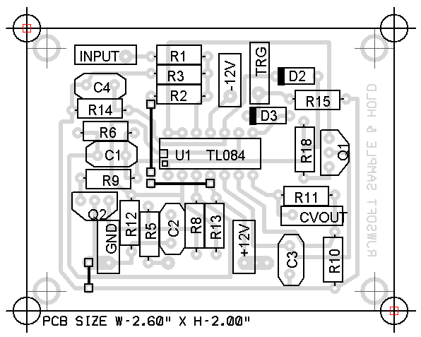
Single Chip Simple Sample and Hold Parts Layout [Parts Layout PDF]
| Notice that you connect one end of the Sample Rate pot to the pad at the end of R5 and the other end of the pot (and the pot wiper) to +V. In the drawing +12V means +V and -12V means -V. You can use between +/- 9V to +/- 15V. |

Single Chip Simple Sample and Hold PC Layout

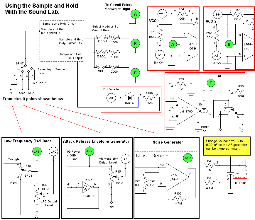
Connecting the Sample and Hold to the Sound Lab
| This diagram shows how I suggest you connect the Sample and Hold to the Sound Lab Mini Synth. |

Single Chip Simple Sample and Hold Parts List
| Qty. | Description | Value | Designators |
|---|---|---|---|
| 1 | TL084 Quad Op Amp | TL084 | U1 |
| 2 | MPF102(s) | MPF102 | Q1, Q2 |
| 2 | High Speed Sw Diode(s) | VALUE | D2, D3 |
| 2 | Ceramic Capacitor (S)(s) | .01uF | C3, C4 |
| 1 | Ceramic Capacitor (S) | 0.2uF | C2 |
| 1 | Ceramic Capacitor (S) | 10pF | C1 |
| 1 | Potentiometer | 1M | R4 |
| 8 | Resistor 1/4 Watt 5%(s) | 100K | R12, R13, R8, R2, R3, R11, R1, R18 |
| 1 | Resistor 1/4 Watt 5% | 10K | R15 |
| 1 | Resistor 1/4 Watt 5% | 150K | R10 |
| 2 | Resistor 1/4 Watt 5%(s) | 1M | R14, R9 |
| 1 | Resistor 1/4 Watt 5% | 360K | R5 |
| 2 | Resistor 1/4 Watt 5%(s) | 3M | R6, R17 |