Voltage Controlled Oscillator and VC-LFO
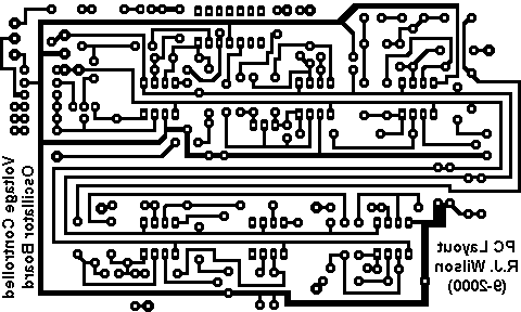
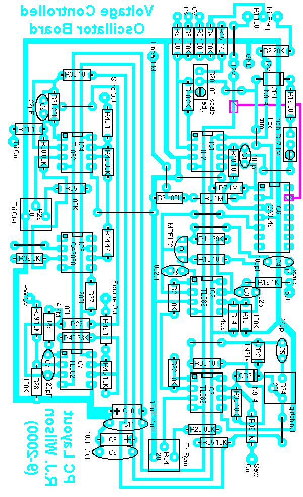
Here is the schematic, PC board layout, and parts placement. Always breadboard first! Have fun.
Voltage Controlled Oscillator and VC-LFO
This is a very cool VCO it puts out sine, triangle, ramp, and pulse waveforms and tracks 1 volt/octave over about 8 octaves or so quite nicely even though it is not temperature compensated. If you have any TEL-LABS Q81s laying about you can directly replace R10 (2K) with one. What I would suggest if you do is that you epoxy it to the CA3046 case and run short leads from it to the PC board mounting holes. The circuit provides sync in and out and you can control the pulse wave's width from about 10% to 90%. All of the parts are very obtainable and not extremely expensive.
IC1A and IC1B and associated components comprise a voltage to current convertor that has a logarithmic relationship. As voltage applied at R3,R5 and R6 goes from 0 to 1 volt the current flowing into pin 5 of the CA3046 goes from approximately 1uA to twice that level (for example 1 uA to 2uA) when the voltage goes from 1 volt to 2 volts the current doubles again (2uA to 4uA). This doubling continues as the voltage continues to increase by 1 volt increments. (for example 3V=8uA,4V=16uA,5V=32uA,6V=64uA,...10V=1024uA). If the current starts at .9uA or 2uA it really doesn't matter what is important is that the current doubles for each increase of one volt in control voltage. The reason the voltage to current relationship is important is that it directly relates to the frequency produced by the oscillator controlled by the current. Your keyboard needs to produce 1/12 of a volt per half step or 83 mV. The V to I convertor produces the logarithmically scaled current. This can be accomplished with a voltage divider or with my MIDI to CV Convertor. I certainly did not invent this method, it is quite ingenious and has been around for some time now.
The heart of the oscillator is formed by IC2A and B. IC2A is an integrator whose output ramps up at a rate that is directly proportional to the current flowing out of its inverting input. IC2B is used as a comparator that causes Q1 to reset the voltage at IC2A's output back to zero. So now we have our control voltage to current convertor and our directly proportional ramp oscillator. The remaining components are used to rectify the ramp (which oscillates about ground) which results in a triangle wave, take the triangle and distort it into a sine wave (using transconductance op amp IC5, and run the triangle through a comparator to square it up (and to provide pulsewidth modulation control).
The sync input just lets you reset the integrator using an external pulse source and the linear modulation allows you to modulate the oscillator frequency with linear response instead of the log response you get at the CV inputs. Syncing two oscillators and then detuning them produces some very cool timbres.
Adjustment and Calibration
I have built several of these and the design and board layout works so if you don't even get oscillation you have a bad part, a short, an open, an incorrect value... something is wrong on your end. After constructing the oscillator and applying power you should see a ramp wave at the output of IC3A. Adjusting R1 should change the frequency of the ramp wave oscillation over a huge range (10 Hz to 18 to 20 Khz). Once you have determined that the ramp portion is functional adjust the output to approximately 1000 Hz. Adjust R24 and R26 until you have a triangle wave which oscillates evenly about ground at pin 1 of IC4A. The output (pin 7) of IC4B should look sinusoidal. Varying the voltage at the "pw CV in" (left side of R29) between approximately -5 volts and approximately 5 volts should vary the duty cycle of the Square/Pulse out between approximately 10% and 90%. Adjusting R34 will eliminate the glitch at the peak of the triangle wave (this is barely if at all audible).
Now adjust R1 so that the oscillator frequency is 60 Hz. You will need to apply a calibrated voltage at one of the CV inputs starting at GND and then increasing the voltage to exactly 1V, 2V, 3V, 4V, 5V... etc. At ground you should have 60 Hz. At 1 volt you should see 120 Hz, at 2V 240 Hz, at 3 volts 480 Hz, at 4 volts 960 Hz, at 5 volts 1920 Hz. OK... you see the pattern each additional volt should result in a doubling of frequency (thus 1V per octave). Adjust R20 so that you get the proper volts/octave response. Adjust R17 to raise the high frequency (> 10KHz) a bit because at high frequency you need the oscillator to give a smidge more than 1 octave per volt response. Use your ears or a frequency counter.
This oscillator is NOT temperature compensated so it will drift. Use it at the same ambient temprerature that you adjusted it at for best results. Does anyone have a good thermostat circuit handy? Please let me know. Mount the R20 and R16 trimmers so that they are accessible from the front panel with a trimmer screw-driver to make your life simpler or you will be behind your synth more than you want to be. OR better yet find a way to temperature compensate this oscillator and let me know about it.
The top to bottom symmetry of the sine wave is related to the R26 (tri offset) adjustment. As you observe the sine wave output on a scope use R26 to set the DC offset of the signal being fed into the CA3080. You will note that the sine wave becomes flatter on top and more triangular on the bottom (or visa versa). Adjust it so that it is symmetrically sinusoidal on top and bottom. If you are unable to adjust the symmetry adequately using R26 you will need to kludge in a 100K pot and 2Meg resistor. Place one end of the pot at +12V and the other at -12V. Attach the resistor between the wiper of the pot and pin 3 of the 3080. Now you will have a separate top to bottom symmetry adjustment pot. If the sine wave is too flat on top and bottom then increase R38 until it looks (and sounds) better. If the sine wave is too triangular on top and bottom then decrease R38 until it looks (and sounds) better.
Changing amplitudes is possible. The ramp is most challenging since the rest of the circuit depends on
it. To change the amplitudes of the waveforms do the following:
- Increase sine wave: Increase value of R43.
- Decrease sine wave: Decrease value of R43.
- Increase triangle: Increase value of R31 (Readjustment of R26 will be necessary)
- Decrease triangle: Decrease value of R31 (Readjustment of R26 will be necessary)
- Increase square: Increase value of R45.
- Decrease square: Decrease value of R45.
- Increase ramp: Increase R22 and R33 (but keep them equal. Affects tri and sine though).
- Decrease ramp: Decrease R22 and R33 (but keep them equal. Affects tri and sine though).
Voltage Controlled Low Frequency Oscillator modification
To use this as a Voltage Controlled Low Frequency Oscillator apply the mods shown on the Voltage Controlled Low Frequency Oscillator Page.Voltage Controlled Oscillator Schematic
This note is from Intersil regarding the CA3046. You will need to kludge in a wire to follow their advice. Also, the most negative point in the circuit is the -12V power supply connection.
NOTES:
1. The collector of each transistor of the CA3046 is isolated from the substrate by an integral diode.
The substrate (Terminal 13) must be connected to the most negative point in the external circuit to
maintain isolation between transistors and to provide for normal transistor action.

VCO PC Board Layout (Component Side View)

This note is from Intersil regarding the CA3046. You will need to kludge in a wire to follow their advice. Also, the most negative point in the circuit is the -12V power supply connection. The kludge is shown below in magenta.
NOTES:
1. The collector of each transistor of the CA3046 is isolated from the substrate by an integral diode.
The substrate (Terminal 13) must be connected to the most negative point in the external circuit to
maintain isolation between transistors and to provide for normal transistor action.
VCO Board Parts Placement Diagram

