Ray Wilson authored this content while he was actively running MFOS as the founder and resident genius.
We retain the content because it reflects a valuable point of view representing that time and place.
Article by Ray Wilson
Features
|
for larger view... |
for larger view... |

Introduction
If you're looking for some new waveforms for your synth you've definitely come to the right place. I have been asked several times to come up with a circuit that takes a basic waveform like a triangle or a sine wave and takes it in a new harmonic rich direction. This circuit takes a triangle or sine wave (or other non-square wave) and allows you to turn it progressively inside out yielding a totally cool sound (peak inversion). Additionally the triangle, sine (or ramp/saw) is converted to what I refer to as a step waveform which has a cool hollow harmonic-rich type of sound. The modified triangle or sine wave output is further enhanced by the addition of a mixer for pulse wave, sub octave square wave and sub-sub octave square wave for very interesting harmonic rich sounds. You'll love the dry sounds you get but when put through a resonant filter your ears will get a real treat. Finally some new waveshapes beyond sine, tri, ramp, saw and square.
Optional Updates
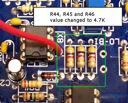
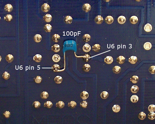
DIYer Peter Kvitek of California brought an observation he made regarding the Wave Freaker's inverted peak waveform to my attention. He noticed switching transisents in the peak inverted wave and helped to determine how to alleviate them. While I had noticed them as well I did not find them objectionable but they were not as pronounced as those he was observing. Bottom line: changing 100K resistors R44, R45 and R46 to 4.7K and adding a 100pF cap between U6 pin 3 and U6 pin 5 (ground) markedly reduces the switching transients. This is not required but it does provide an improvement in the quality of the folded peak waves. Since this is an optional change the parts list still reflects the original values. If you want to incorporate this change, order 3 additional 4.7K 1/4W 5% resistors and 1 small 100pF cap.
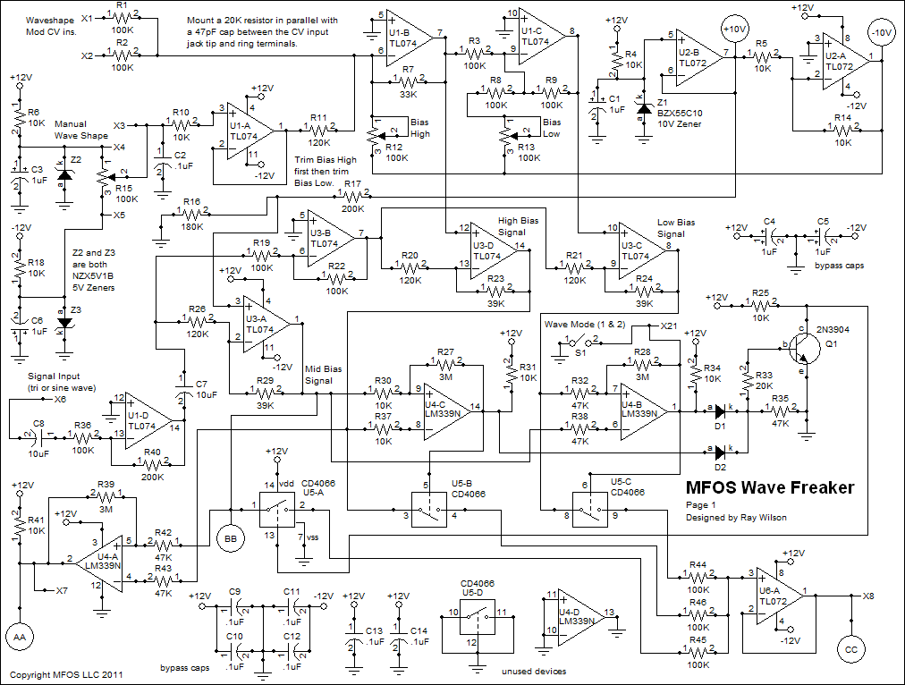
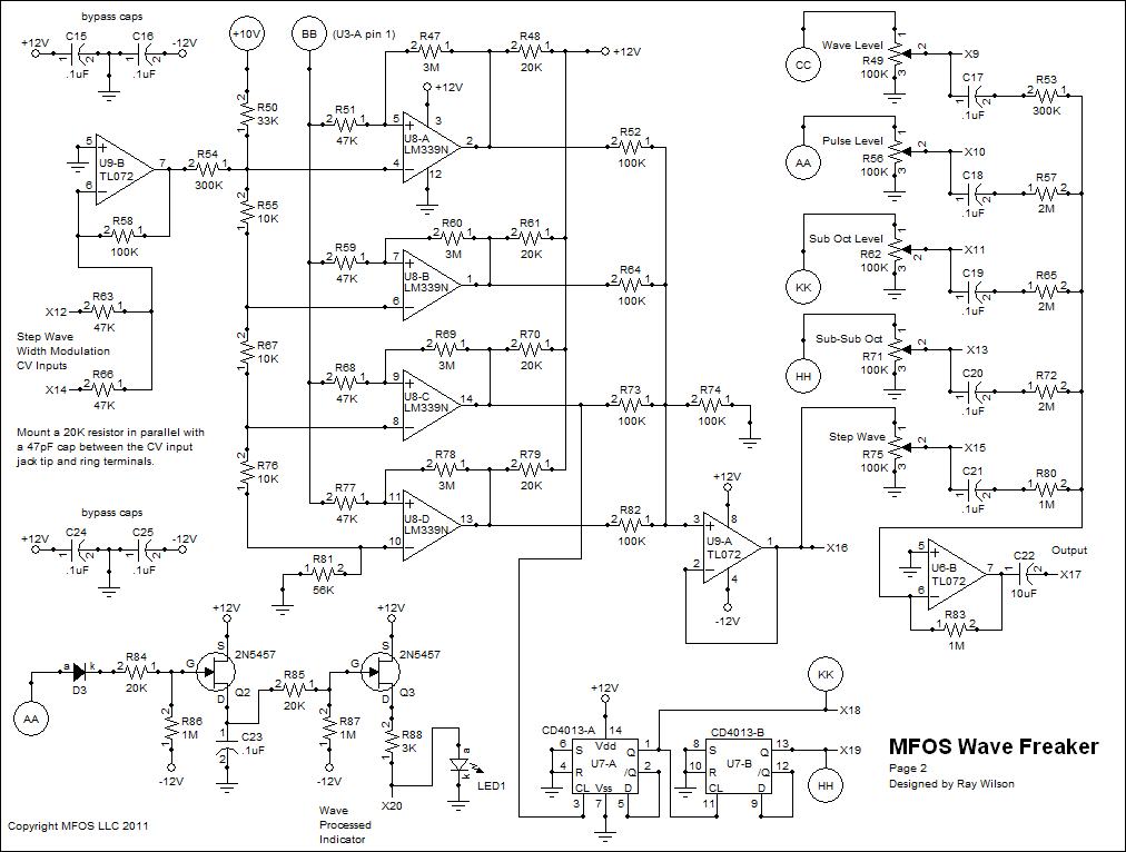
Wave Freaker Schematic Page 1
View as PDF
Circuit Description
We'll start by discussing the bias generation for the circuit. The 5V zener diodes Z2 and z3 are connected to produce plus and minus 5V levels to apply to the ends of the manual waveshape knob. I tried to keep all biasing zener based to alleviate any issues related to power supplies. However the circuit must be run on a minimum +/-12V supply. Resistors R6 and R18 are current limiters for the zeners. C3 and C6 are both there to keep the voltage at the ends of R15 (100K linear pot) clean and quiet. the wiper of R15 connects to the input of U1-A (TL074) used as a gain of 1 buffer amp. C2 (.1uF ceramic cap) quiets any reflected signals on the wire from the wave shape pot to the PCB. As pot R15 is adjusted from end to end the output of U1-A goes from approximately -5V to +5V which is the expected level of maximum CV input as well. The output of U1-A is fed via R11 (120K resistor) to the summing node of inverting op amp U1-B. U1-B serves as an inverting summer for the CV input voltages as well as the voltage from the manual wave shape pot (R15). The output of U1-B (TL074) goes to the inverting input of U1-C (TL074) via R3 100K 1% resistor. U1-C's feedback resistor (R9) gives U1-C a gain of -1.
U1-B inverts the CV and manual wave shape pot voltages arriving at it's inverting input and U1-C re-inverts the voltages so that U1-C mirrors the voltage at U1-B pin 7. As the voltage on U1-B pin 7 output goes low in response to increasing control voltage the output of U1-C goes high equally and simultaneously. U2 in conjunction with Z1 (10V zener) is used to generate +/-10V which is used for biasing throughout the circuit. Both U1-B and U1-C use the -10V bias level generated at the output of U2-A to set the initial bias levels for U3-D and U3-C respectively.
The signal level arriving at X6 comes from the wiper of the 100K Input Level pot (no designator but shown on the wiring diagram). The input is AC coupled via C8 to the input signal buffer amplifier U1-D (TL074). U1-D's output is capacitiviely coupled to the inputs of both U3-A and U3-B via their respective gain set resistors (R26 and R19). With no signal input the biasing on the non-inverting input of U3-A (Tl074) causes it's output to sit at about 5.3 volts. This causes it's non-inverting input to sit at the same voltage and C7 charges to this level. Thus the inverting input of U3-B (TL074) inverting gain of 1 amplifier sees the same DC voltage. Thus U3-B's output has a negative offset equal but opposite to the voltage seen at the junction of C7, R26 and R19. The output of U3-B feeds the inverting inputs of U3-D and U3-C. Both of these op amps have a gain of about -1/3 (which is the same gain as U3-A).
With the Input Level and Wave Shape pots both set fully counterclockwise we now measure and set the bias levels on the outputs of U3-D and U3-C. ALWAYS SET R12 FIRST! Observe the voltage level on the output of U3-A and remember it (call it x). While observing the DC level on the output of U3-D (pin 14) adjust R12 (Bias High trimmer) until you measure x + 3 volts there. While observing the DC level on the output of U3-C (pin 8) adjust R13 (Bias Low trimmer) until you measure x - 3 volts there.
Between the Input Level pot and the fact that U1-D (input signal buffer op amp) provides a gain of two the input can accept a wide range of signal levels. Ideally you want to see about +/-5V on the output of U1-D and to reiterate use a sine or triangle wave signal as input.
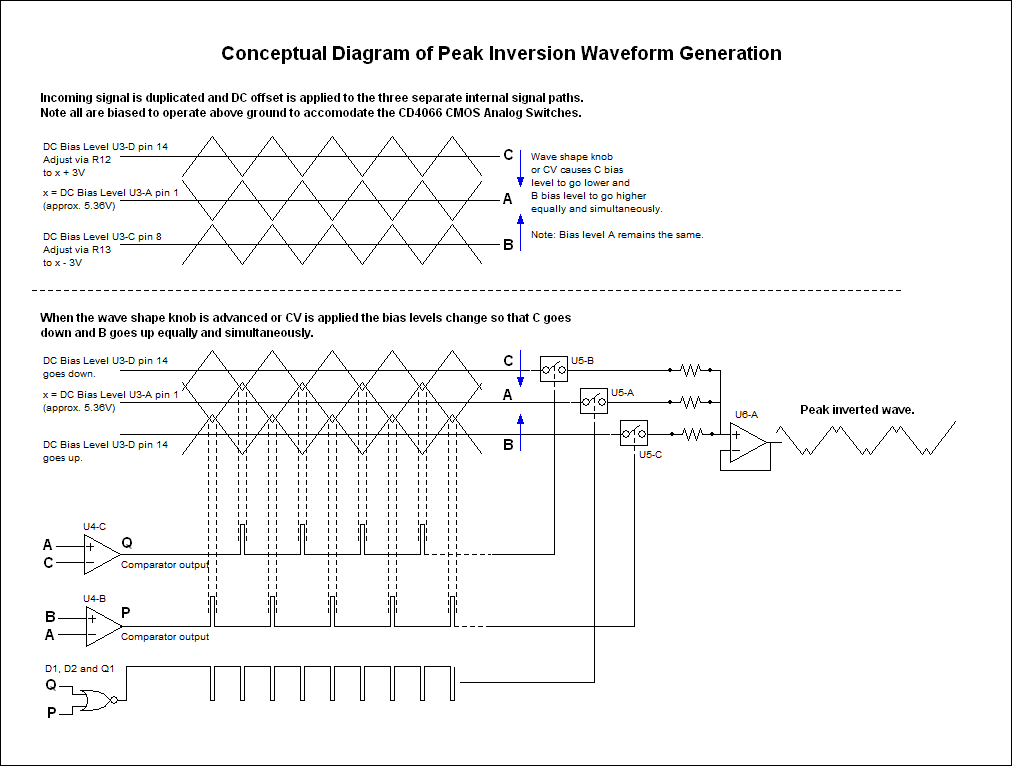
Now the triangle or sine wave signal we have input appears on the outputs of: U3-A (pin 1) riding on a bias of about 5.3V, U3-D (pin 14) riding on a bias level of about 8.3V, and U3-C (pin 8) riding on a bias level of about 2.3V. The +/-5V signal appearing at the output of U1-D (pin 14) is reduced in amplitude by a factor of 3 by all three op amps (U3-A, U3-D and U3-C) by their input (120K) and feedback (39K) resistors. This puts the AC levels on their outputs at about 3.3V peak to peak. The reason we bias all of the outputs to be above ground is so we can use the CD4066 analog switch later in the signal processing. Since the CD4066 is powered by V+ and ground it's analog switches can only pass positive level signals. Negative level signals on the inputs of the CD4066 will turn on the parasitic protection diodes and cause havoc (and excessive current drain).
The bias levels on the non-inverting inputs of U3-D and U3-C are controlled simultaneously by both the Wave Shape pot and the control voltage inputs. As the Wave Shape pot is advanced or the CV voltage is raised from -5V toward +5V the bias level on the output of U3-D goes lower and the bias level of U3-C goes higher due to the action of op amps U1-B and U1-C. Their bias levels change the same amount but in opposite directions.
Bear in mind that the AC signals on the outputs of U3-D and U3-C are an inverted version of the output of U3-A so the valleys of the triangle signal appearing at the output of U3-A correspond to the peaks of the signal apearing at the outputs of both U3-D and UI3-C and vice versa. The purpose of this is so that as the bias levels on the outputs of U3-D and U3-C change (U3-D bias goes lower and U3-C bias goes higher) the signal voltages on the outputs intersect (voltage wise). This results in the voltage level of the valleys of the signal on the output of U3-D going below the voltage level of the peaks of the signal on the output of U3-A and the voltage level of the peaks of the signal on the output of U3-C going above the voltage level of the valleys of the signal on the output of U3-A. Now on to the comparators...
We detect the intersections of these voltages with comparators. We're using the LM339 quad comparator for this application. I have to say that I was impressed at the improvement in speed comparators provide regarding rise and fall times. I use op amps as comparators in many circuits and they work fine but when you need fast rise or fall times pick a comparator chip specifically. U4-C (LM339 comparator) is used to compare the outputs of U3-A and U3-D. When the voltage on the output of U3-A goes above the voltage on the output of U3-D the output of U4-C which is normally low (sinking current to ground) is pulled high rapidly by resistor R31 (10K). U4-B (LM339 comparator) is used to compare the outputs of U3-A and U3-C. When the voltage on the output of U3-A goes below the voltage on the output of U3-C the output of U4-B which is normally low (sinking current to ground) is pulled high rapidly by resistor R34 (10K). When either of the comparator outputs is high Q1 (2N3904 NPN transistor) is turned on via high speed diodes D1 or D2 sending current to it's base via R33. When Q1 is on it's collector pulls to ground (goes low). When both of the outputs of the comparators are low Q1 is turned off by R35 to ground and it's collector pulls high via R25 (10K resistor).
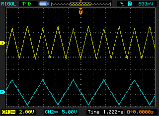
When the outputs of both U4-C and U4-B are low and the collector of Q1 is pulled high by R25 (10K resistor) CD4066 analog switch U5-A is turned on and passes the signal from the output of U3-A to the non-inverting input of U6-A (non-inverting buffer) via R45 100K resistor. Components D1, D2, R33, R35, Q1 and R25 comprise a NOR gate function. When the output of U4-C is high CD4066 analog switch U5-B is turned on and passes the signal from the output of U3-D to the non-inverting input of U6-A (non-inverting buffer) via R46 100K resistor. When the output of U4-B is high CD4066 analog switch U5-C is turned on and passes the signal from the output of U3-C to the non-inverting input of U6-A (non-inverting buffer) via R44 100K resistor. The composite signal appearing at the output of U6-A is the inverted peak signal. That is a signal that changes direction as it approches it's positive and negative peak levels. As the peaks are inverted earlier and earlier (Wave Shape knob is turned up) the signal progressively gains a heavy fifth above the octave harmonic and sounds very interesting when you are in dual peak invert Wave Shaper mode. In single peak invert Wave Shaper mode the signal gains a strong octave harmonic as the Wave Shape knob is advanced.
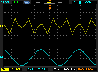
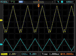
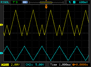
| Blue - input triangle wave. Yellow shows the Wave just as it begins to be peak inverted. | Blue - input triangle wave. Yellow shows more peak inversion. | Blue - input triangle wave. Yellow shows wave almost inside out. | |||
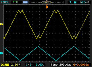 |  | 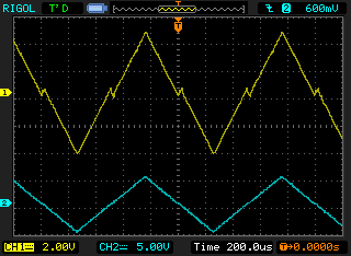 | |||
| Blue - input sine wave. Yellow shows the Wave just as it begins to be peak inverted. | Blue - input sine wave. Yellow shows more peak inversion. | Blue - input sine wave. Yellow shows wave almost inside out. | |||
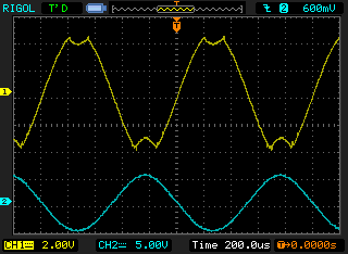 |  | 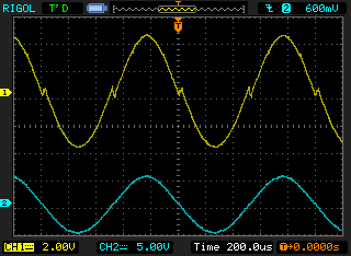 | |||
Switch S1 can be used to disable the output of U4-B from going high and turning on U5-C so that only one peak is inverted. As the single peak is inverted earlier and earlier (Wave Shape knob is turned up) the signal progressively gains a heavy octave harmonic and again sounds very interesting. Don't freak about shorting the output of U4-B to ground. Remember that it's output is an NPN transistor collector that normally pulls the output to ground. It's output only goes high because we pull it high with the 10K pull-up resistor R34. So when we short the output we are only shorting the junction of U4-B pin 1 and the 10K resistor connected to it's output to ground.
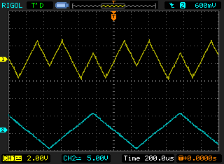
| Blue - input triangle wave. Yellow shows the Wave just as it begins to be single peak inverted. | Blue - input triangle wave. Yellow shows more single peak inversion. | Blue - input triangle wave. Yellow shows more single peak inversion. | |||
 |  |  | |||
We also compare U3-A's output and U3-D's output to generate a pulse waveform when their voltage levels intersect. This pulse waveform is applied to the output mixer via Pulse Level pot R56 to add additional harmonics to the output waveform. This wave will be pulse width modulated more or less as the voltage levels intersect. It should be noted that if the voltage levels are not intersecting due to Input Level low or Wave Shape turned completely counter clockwise the pulse wave will not occur.
All of the comparators used have positive feedback to provide hysteresis (3M resistor between non-inverting input and output). This helps the comparators switch cleanly. One of the great features of the LM339 is it's ability to detect as low as 2mV difference between the inputs but when wired like that any tiny noise will interfere with the transition causing chatter. I chose to go with more hysteresis (3M feedback resistors) because when I tried 10M feedback resistors it was too noisy during transitions.
Bypass caps (.1uF and 1uF) are used throughout and are placed as close as practicable to the chips on the PCB. The circuit points in the circles are simply intra or inter-page connection indicators. Points AA, BB, CC and +10V all continue on schematic page 2. I use them to connect points on the same page if connecting everything normally becomes too crowded and/or hard to read.
Peak Inversion Conceptual Diagram
View as PDF
Description
I think this diagram in concert with the circuit description above will help cement the concepts of what's going on in this circuit to achieve the wave peak inversion function.
Wave Freaker Schematic Page 2
View as PDF
Circuit Description
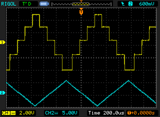
The step waveform generator takes the output from U3-A (circuit point BB) and applies it to the non-inverting inputs of a group of 4 comparators. The inverting inputs are tied to a resistor string that uses the +10V generator from page 1 to create equally spaced voltage steps that start at about 4.1V on pin 10 of U8-D and go to about 6.3V on pin 4 of U8-A. When the signal from U3-A pin 1 is above the level on any comparator's inverting input the output of that comparator goes high. Since the triangle, sine, ramp or sawtooth wave on the output of U3-A goes from slightly below the first reference and progressively up until it is slightly above the highest reference the comparator outputs go high successively as each threshold is crossed. The outputs are summed so that as more comparators go high the output of U9-A (used as the non-inverting summer) steps higher and then as more comparators go low the output steps down. It's a cool way to get a very freaky looking and sounding waveform. The output of the step wave generator buffer amp U9-A (TL072) is fed to the mixer via potentiometer R75 Step Wave Level pot.
U9-B is the Step Wave width modulation control voltage input summer and as control voltage is applied to it's inputs via R63 and/or R66 (both 47K resistors) the voltage reference on the inverting inputs of the comparators is changed which affects the width of mainly the top and bottom steps of the step wave. The modulation can cause the top and bottom steps to be clipped completely which has a unique sound as well.
| Blue - input triangle wave. Yellow - Resulting Step wave. | Blue - input since wave. Yellow - Resulting Step wave. | Blue - input ramp wave. Yellow - Resulting Step wave. | |||
 | 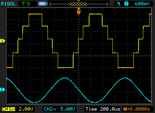 |  | |||
One of the mid-level comparator outputs (U8-C pin 14) feeds the clock input of CD4013's flip flop A. We use this flip flop to generate both the Sub-Octave and the Sub-Sub-Octave square waves. On the low to high transition of the clock the data on the D input is latched to the Q output. So whatever logic level was sitting on the NOT-Q goes to the Q and the not Q goes to the opposite level. This action causes the flip flop to essentially divide the clock frequency in half. The Q output of U7-A is fed both to the 100K audio taper mixer pot R62 and the clock input of U7-B to generate the sub-sub-octave signal. U7-B's Q output is fed to the 100K audio taper mixer pot R71.
To give a visual indication of when the circuit's internal waveform voltages begin to intersect the output of comparator U4-A, which compares the signals from U3-A and U3-D, is fed to the kathode of D3. When no positive excursions are occurring on the output of comparator U4-A (no waveform voltage intersection), 1M resistor R86 holds the gate of Q2 at -12V essentially turning it completely off. The positive excursions of the signal at the output of U4-A (waveform voltages intersecting) forward bias D3 and turns on Q2 (2N5457 N-Channel JFET) via current through 20K resistor R84 causing Q2 to pass current from source to drain and charge C23 from the +12V supply. The voltage on C23 applied to the gate of Q3 (2N5457 N-Channel JFET) subsequently turns on Q3 and allows current to flow through the transistor and 3K current limiting resistor R88 to illuminate LED1. This scheme is used because even narrow pulses applied to point AA will light the LED completely.
Finally the mixer itself uses U6-B as a simple inverting summer. The audio taper 100K mixer pots (R49, R56, R62, R71, R75) are used as adjustable voltage dividers whose wipers feed 0.1uF ceramic AC coupling capacitors (C17, C18, C19, C20, and C21) and mixer resistors (R53, R57, R65, R72, and R80). The level adjusted signals are summed by U6-B the output of which is capacitively coupled to the output jack via 10uF bipolar capacitor C22. I feel that the output level is sufficient but if your gear needs more gain it is a simple matter of increasing the value of R83. Taking it to 2M will double the output level for example.
The circuit draws about 39 mA (LED on, 36 mA LED off) from the +12V supply and about 28 mA from the -12V supply.
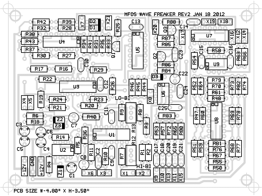
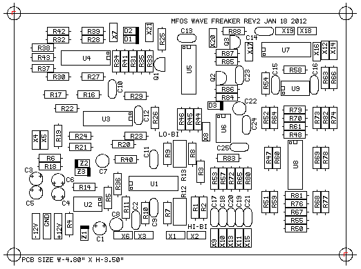
PC Board Component Designators
View as PDFThis view is good during trouble shooting since that's when you normally search for designators on the PCB and many designators are obscured by the installed components.
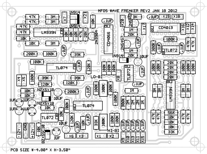
PC Board Component Values
View as PDFThis view is good during board population so you don't have to continually refer back and forth to the schematic to find component values.
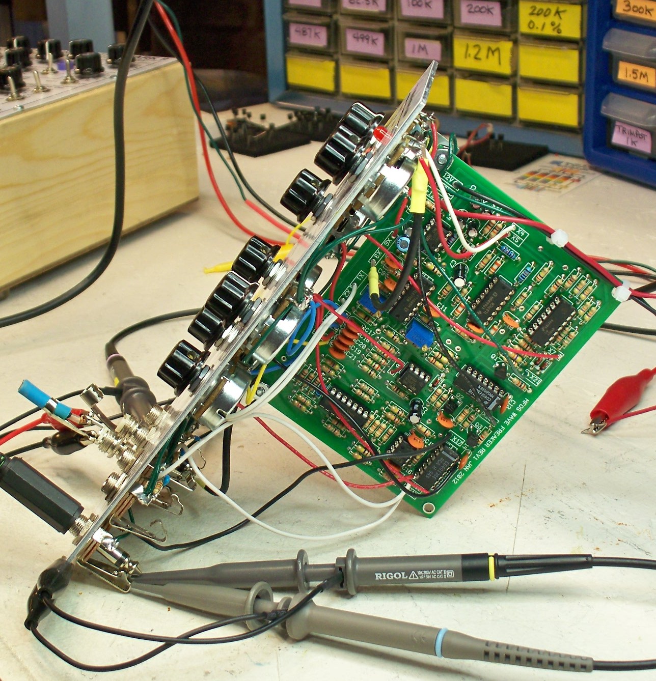
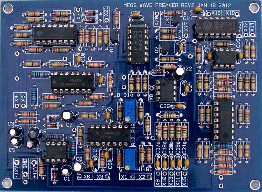
PC Board Populated
Populated production board. I ended up making this three times. Once for the original prototype, again for prototype number two and yet again for the production board. I never sell em' until I build and test em'. Prototype number two worked perfectly. I just moved a couple of components around and added two more bypass caps. I plan to have at least two of these babies in my modular.
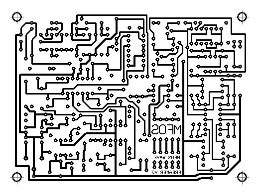
PC Board Bottom Copper
To get these to the correct size experiment with the dots per inch output of your drawing program. When the IC socket footprint lines up with an integrated circuit you have the right scale.
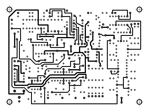
PC Board Top Copper
PC Board Designators Silk Screen
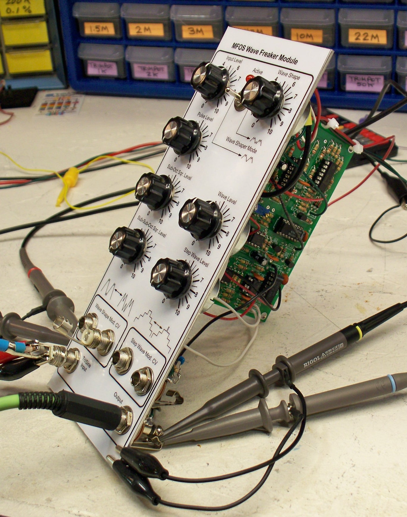
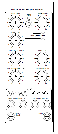
Front Panel Suggestion
View as PDFThis is just a suggestion whose purpose is simply to relate to the wiring diagram. Use your creativity and create your own cool panel but remember to draw an accompanying wiring diagram so you don't make panel wiring errors.
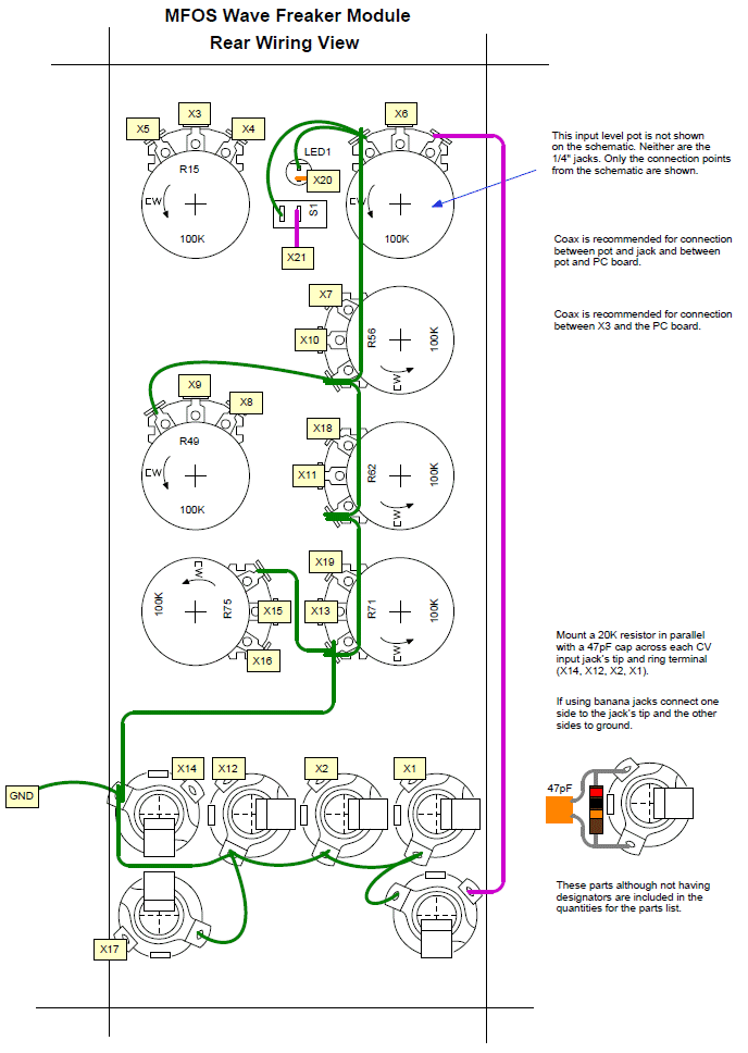
Front Panel Wiring
View as PDFThis wiring relates to the suggested front panel drawing.
MFOS Wave Freaker Project Parts List
Project Parts List
NOTE! The zener diodes do not have to be the exact part number as long as they are the correct voltage and 0.5W.
| Qty. | Description | Value | Designators |
|---|---|---|---|
| 1 | CD4013 Dual D Flip Flop | CD4013 | U7 |
| 1 | CD4066 | CD4066 | U5 |
| 2 | LM339N Quad Comparator | LM339N | U4, U8 |
| 3 | TL072 Dual Op Amp | TL072 | U2, U6, U9 |
| 2 | TL074 Quad Op Amp | TL074 | U1, U3 |
| 2 | Transistor NFET 2N5457 | 2N5457 | Q2, Q3 |
| 1 | Transistor NPN 2N3904 | 2N3904 | Q1 |
| 3 | Diode 1N914 | 1N914 | D1, D2, D3 |
| 1 | Diode 10V 0.5W Zener BZX55C10 | BZX55C10 | Z1 |
| 2 | Diode 5V 0.5W Zener NZX5V1B,133 | NZX5V1B | Z2, Z3 |
| 1 | LED | LED | LED1 |
| 6 | Potentiometer Audio Taper | 100K | R49, R56, R62, R71, R75 (1 for input level control) |
| 1 | Potentiometer Linear | 100K | R15 |
| 2 | Potentiometer Multi-turn Trimmer (top adjust) | 100K | R12, R13 |
| 2 | Resistor 1/4 Watt 1% | 10K | R5, R14 |
| 4 | Resistor 1/4 Watt 1% | 100K | R3, R9, R19, R22 |
| 4 | Resistor 1/4 Watt 5% | 120K | R11, R20, R21, R26 |
| 1 | Resistor 1/4 Watt 5% | 180K | R16 |
| 4 | Resistor 1/4 Watt 5% | 1M | R80, R83, R86, R87 |
| 2 | Resistor 1/4 Watt 5% | 200K | R17, R40 |
| 11 | Resistor 1/4 Watt 5% | 20K | R33, R48, R61, R70, R79, R84, R85 (4 mounted across tip/ring of CV jacks) |
| 3 | Resistor 1/4 Watt 5% | 2M | R57, R65, R72 |
| 2 | Resistor 1/4 Watt 5% | 300K | R53, R54 |
| 2 | Resistor 1/4 Watt 5% | 33K | R7, R50 |
| 3 | Resistor 1/4 Watt 5% | 39K | R23, R24, R29 |
| 1 | Resistor 1/4 Watt 5% | 3K | R88 |
| 7 | Resistor 1/4 Watt 5% | 3M | R27, R28, R39, R47, R60, R69, R78 |
| 11 | Resistor 1/4 Watt 5% | 47K | R32, R35, R38, R42, R43, R51, R59, R63, R66, R68, R77 |
| 1 | Resistor 1/4 Watt 5% | 56K | R81 |
| 13 | Resistor 1/4 Watt 5% | 100K | R1, R2, R8, R36, R44, R45, R46, R52, R58, R64, R73, R74, R82 |
| 13 | Resistor 1/4 Watt 5% | 10K | R4, R6, R10, R18, R25, R30, R31, R34, R37, R41, R55, R67, R76 |
| 3 | Capacitor Alum. Nonpolarized | 10uF | C7, C8, C22 |
| 17 | Capacitor Ceramic | .1uF | C2, C9, C10, C11, C12, C13, C14, C15, C16, C17, C18, C19, C20, C21, C23, C24, C25 |
| 5 | Capacitor Electrolytic | 1uF | C1, C3, C4, C5, C6 |
| 4 | Capacitor Ceramic | 47pF | Mounted across tip/ring of CV jacks |
| 1 | Mini Toggle Switch SPST | SPST | S1 |
| 6 | Jacks of your choice | Jacks | Jacks for all input/output connections. |
| 7 | Pot knobs | Knobs | Knobs for all potentiometers. |