Ray Wilson authored this content while he was actively running MFOS as the founder and resident genius.
We retain the content because it reflects a valuable point of view representing that time and place.
Article by Ray Wilson
While recently building six units I discovered that the value of C5 used in the manual gate pushbutton circuit should be changed to .1uF to provide adequate manual gate switch debouncing. At minimum ADR times the manual pushbutton was bouncing (triggering more than one ADSR cycle). By replacing C5 (formerly .01uF) with .1uF the manual pushbutton worked properly even at minimum ADR times.
Another optional change is to make R25 a 200 ohm resistor instead of 1K. This shortens the minimum ADR times a bit if that is something you would prefer.
Features
- 1 mS to 20 second Attack, Decay, and Release times.
- Classic ADSR envelope shape and functionality.
- Gate and trigger inputs permit retrigger after Attack complete.
- Comparators on gate and trigger inputs.
- Power Supply Range +/-9V up to +/-15V
Introduction
Envelope generators provide a source of voltage that is shaped like a common amplitude envelope. The gate input is used to initiate the ADSR envelope. The following assumes the gate is maintained throughout the attack, decay and sustain cycles. The voltage envelope rises from 0V to 10 volts during the attack cycle at the rate set by the Attack control. At the peak of the attack cycle (10 volts) the decay cycle is entered. The voltage decays to the sustain level (0 to 10 volts dependant on the setting of the Sustain control) at the rate determined by the Decay control. When the gate is released the release cycle is entered and the voltage decays to 0 at the rate determined by the Release control setting. If the gate is removed at any time during the A,D or S cycle the release state is immediately entered. The trigger input used alone can initiate an attack release cycle. When used in conjunction with the gate the trigger can re-initiate an attack cycle when it occurs during the decay or sustain cycles.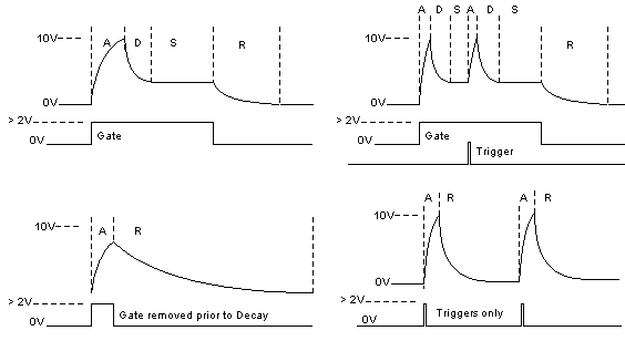
ADSR Envelope Generator Page 1 PDF
|
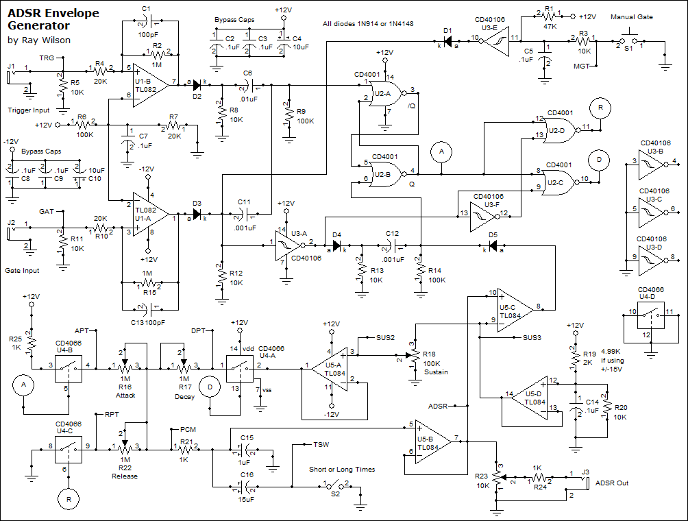
With gate and trigger inputs at 0V the circuit is at its quiescent state. Point R is high in this state because both inputs of U2-D are low. Point R being high causes analog switch U4-C to be on which discharges C15 to ground via the Release pot's resistance setting. When the gate input is brought slightly above 2 volts the comparator comprised of U1-A and associated components goes from -V to +V very quickly. This pushes current through C11 and drops a high going spike across R9. The spike across R9 causes the flip-flop comprised of U2-A and U2-B to output a high logic level on pin 4 of U2-B. This high level turns off analog switch U4-C and turns on analog switch U4-B which begins to charge C15 (or C15 and C16 in parallel if S2 is closed) toward V+. The voltage on C15 is sensed by U5-C which acts as a comparator with a threshold of 10 volts. When C15 charges to 10 volts U5-C's output goes from -V to +V very quickly. The positive excursion of the output of U5-C (pin 8) is fed to the input of U2-B via D5 and causes the flip-flop comprised of U2-A and U2-B to output a low logic level on pin 4 of U2-B. The presence of the gate keeps U2-D's output low but also allows U2-C's output to go high turning on U4-A which allows C15 to discharge to the level of U5-A's output (which is determined by the sustain pot setting). When the gate is released C15 is discharged to ground at the rate set by the Release pot when analog switch U4-C closes. If the gate is applied and release before the decay cycle the output of U3-A goes high and resets the flip-flop comprised of U2-A and U2-B so that the release phase is entered immediately. Application of trigger pulses (along with the gate present) after the attack phase has completed sets the flip flop and starts the attack cycle over again. Application of trigger pulses (without the gate present) results in a complete attack phase followed by the release phase. |
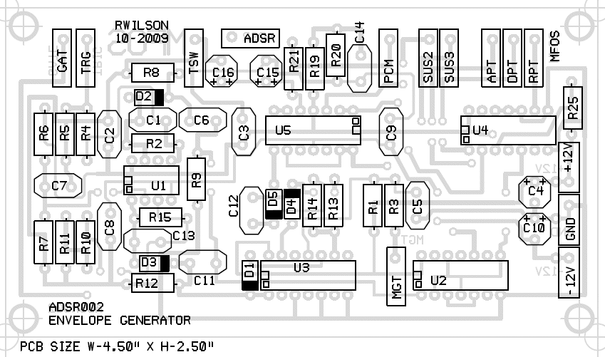
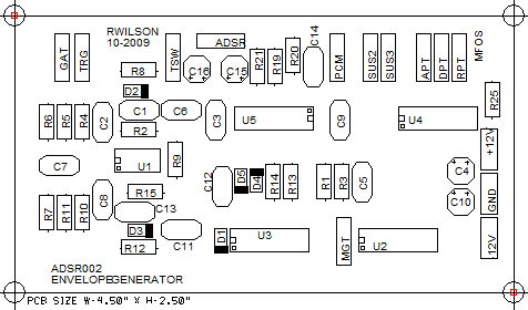
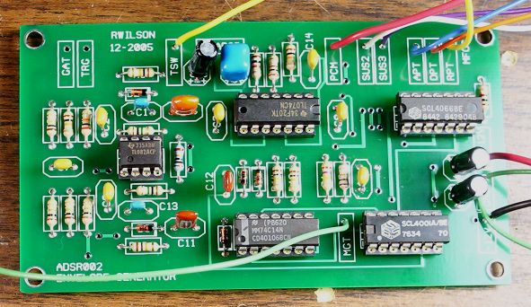
ADSR Envelope Generator PCB Parts Layout (Parts Side Shown) PDF
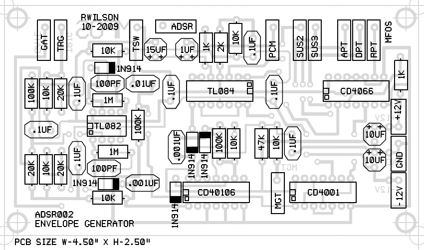
ADSR Envelope Generator PCB Part Value View (Parts Side Shown) PDF
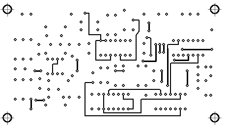
ADSR Envelope Generator PCB Bottom Copper (Parts Side Shown)
4.22" between horizontal targets. 2.22" between vertical targets.
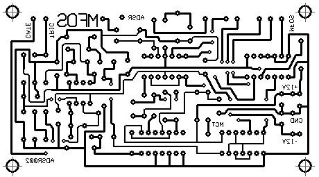
ADSR Envelope Generator PCB Top Copper(Parts Side Shown)
4.22" between horizontal targets. 2.22" between vertical targets.
ADSR Envelope Generator PCB Top Silk Screen
ADSR Envelope Generator Front Panel Suggestion PDF
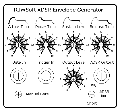
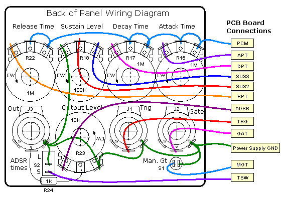
ADSR Envelope Generator Front Panel Wiring PDF
ADSR Envelope Generator During Testing
ADSR Envelope Generator Project Parts List
| Qty. | Description | Value | Designators |
|---|---|---|---|
| 1 | CD4001 Quad NOR | CD4001 | U2 |
| 1 | CD40106 | CD40106 | U3 |
| 1 | CD4066 | CD4066 | U4 |
| 1 | TL082 Dual Op Amp | TL082 | U1 |
| 1 | TL084 Quad Op Amp | TL084 | U5 |
| 5 | 1N914 Sw. Diode | VALUE | D1, D2, D3, D4, D5 |
| 1 | Potentiometer | 100K | R18 |
| 1 | Potentiometer | 10K | R23 |
| 3 | Potentiometer | 1M | R16, R17, R22 |
| 3 | Resistor 1/4 Watt 5% | 100K | R6, R9, R14 |
| 7 | Resistor 1/4 Watt 5% | 10K | R3, R5, R8, R11, R12, R13, R20 |
| 3 | Resistor 1/4 Watt 5% | 1K | R21, R24, R25 |
| 2 | Resistor 1/4 Watt 5% | 1M | R2, R15 |
| 3 | Resistor 1/4 Watt 5% | 20K | R4, R7, R10 |
| 1 | Resistor 1/4 Watt 5% | 2K | R19 |
| 1 | Resistor 1/4 Watt 5% | 47K | R1 |
| 2 | Ceramic Capacitor | .001uF | C11, C12 |
| 1 | Ceramic Capacitor | .01uF | C6 |
| 7 | Ceramic Capacitor | .1uF | C2, C3, C5, C7, C8, C9, C14 |
| 2 | Ceramic Capacitor | 100pF | C1, C13 |
| 2 | Electrolytic Capacitor | 10uF | C4, C10 |
| 1 | Electrolytic Capacitor | 15uF | C16 |
| 1 | Electrolytic Capacitor | 1uF | C15 |
| 1 | SPST PB Switch | SPST | S1 |
| 1 | SPST Switch | SPST | S2 |
| 3 | Jack (2 Conductor) | jack | J1, J2, J3 |
Miscellaneous
- (1) 4" x 10" 1/16" thick Aluminum plate for mounting the pots and switches.
- Unit is typically mounted in a synth case with other synth modules.
- Assorted hardware 1" 6-32 nuts and bolts, 1/2" #8 wood screws, etc
- Knobs for potentiometers, wire, solder and typical assorted electronics hand tools.
- Digital Volt Meter and a Signal Tracer or oscilloscope for testing.