Ray Wilson authored this content while he was actively running MFOS as the founder and resident genius.
We retain the content because it reflects a valuable point of view representing that time and place.
Article by Ray Wilson
Features
|
Introduction
VCAs are essential to your synthesizer. They provide ring modulation effects, stereo panning, delayed vibrato, not to mention the normal envelope shaping of your sounds. This VCA works nicely with 10V PP (+/-5V) signal levels. If you are using +/-15 volt supplies you will probably need to mess with some values to get this to work for you.
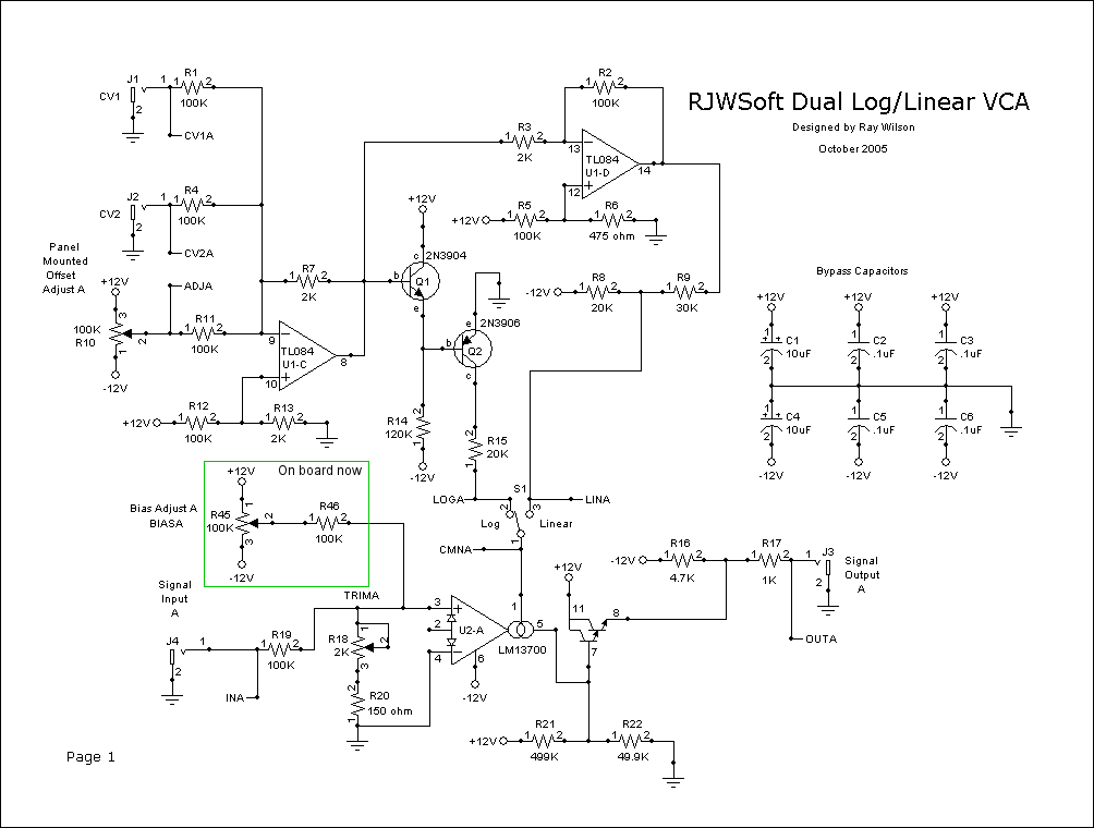
Dual Log/Linear VCA Page 1 PDF
|
This VCA uses the LM13700 transconductance amplifier as the gain control cell. The input voltage is converted to a log response by U1-C and associated transistors Q1 and Q2. The summed control voltage appearing at the output of U1-C is sent to U1-D for reamplification and application to the LM13700 via R9 and S1. S1 selects the current generated by either the log version of the input voltage (LOGA on the schematic) or the linear version (LINA on the schematic) and applies it to the "amp bias in" pin 1 of the LM13700 thus controlling the current through the device and subsequent amplitude of the resulting voltage generated across R16. The LM13700's built in buffers are used to drive the output. They work quite well. The Offset adjust is used to null the gain for whatever control voltage you are using to drive the VCA. You must readjust the null when you switch from log to linear (or visa versa). I have noticed that for control signals that are operating about ground (i.e. + and - 4 to 5 volts) the pot is usually toward the left when set to linear response and usually toward the right when set to exponential response. The TRIMA control is used to set the voltage divider which feeds the non-inverting input of the LM13700 (pin 3). Adjust it for 50mV peak to peak signal at the maximum input voltage. It permits adjustment so that voltage from about + and - 3VPP to + and - 5VPP can be accommodated. You can use just about any general purpose quad BIFET opamp for the TL084 and you can sub any of these (LM13600, NE5517, AU5517, NTE870) for the LM13700. Just in case you are wondering, I have tried to use the bias inputs to forward bias the distortion reducing diodes in the chip but always find that it completely bugs up the biasing throughout the circuit. Bias Adjust (on-board no-kludge now!) If you use an alternate chip or you notice that the output signal is biased high or low you can adjust the ratio of R21 and R22 or add the bias adjust components (R45, R46, R47, R48) I show in green boxes on the schematics. You can add the components to either or both of the VCA circuits if you need to. I did not need to add these components but I did have to select a second LM13700 from my parts drawer because the first one was either defective or the amps on the chip were not well matched. Under normal (i.e. reasonably matched transconductance amps) circumstances you should not need the bias adjust components. |
Dual Log/Linear VCA Page 2 PDF
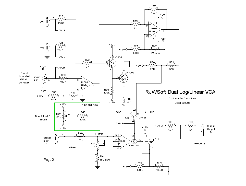
| Page 2 is the same as page one but with different part designators. |
|
Triangle Wave Modulation in Linear Mode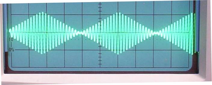 |
|
Triangle Wave Modulation in Log Mode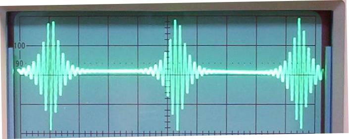 |
|
The Prototype Being Tested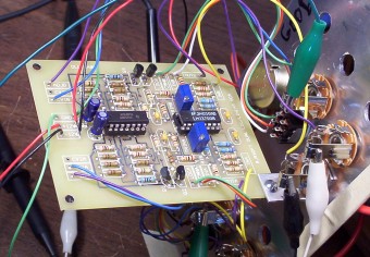
|
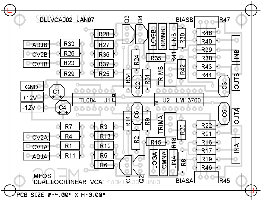
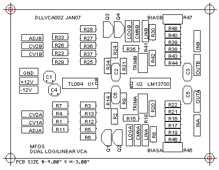
Dual Log/Linear VCA PCB Parts Layout (Parts Side Shown) PDF
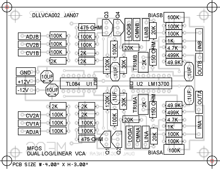
Dual Log/Linear VCA PCB Part Values View (Parts Side Shown)
Dual Log/Linear VCA PCB Bottom Copper (Parts Side Shown)
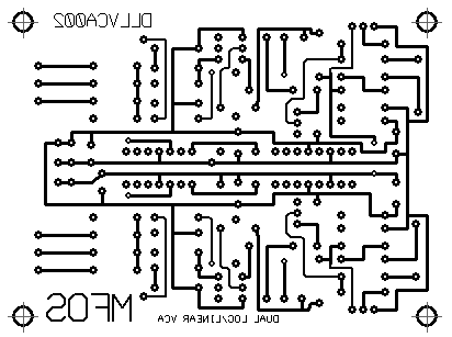
Dual Log/Linear VCA PCB Top Copper(Parts Side Shown)
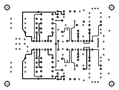
Dual Log/Linear VCA PCB Top Silk Screen
Dual Log/Linear VCA Front Panel and Wiring PDF
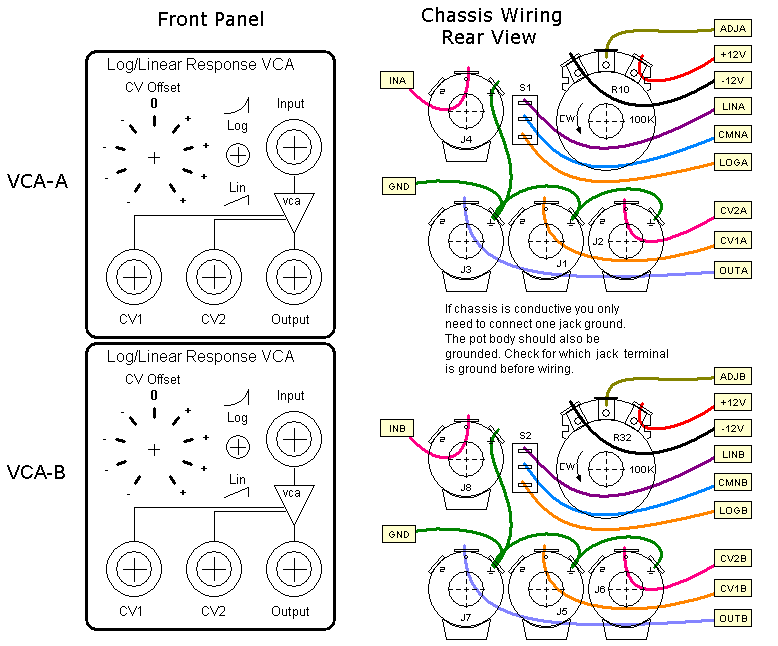
| Jason Proctor took the time to make a nice Front Panel Express design and share it with all of us. If you use it make sure you take into account any differences related to the wiring diagram. | ||
|
Dual Log/Linear VCA Project Parts List
| Qty. | Description | Value | Designators |
|---|---|---|---|
| 2 | 2N3904(s) | 2N3904 | Q1, Q3 |
| 2 | 2N3906(s) | 2N3906 | Q2, Q4 |
| 1 | TL084 Quad Op Amp | TL084 | U1-C, U1-D, U1-B, U1-A |
| 1 | LM13700 Dual gm OpAmp | LM13700 | U2-A, U2-B |
| 2 | Linear Pot(s) RS 271-092 | 100K | R10, R32 |
| 2 | Trim Pots | 100K | R47, R45 |
| 16 | Resistor 1/4 Watt 5%(s) | 100K | R1, R11, R2, R5, R4, R12, R19, R23, R33, R27, R26, R40, R36, R24, R46, R48 |
| 2 | Resistor 1/4 Watt 5%(s) | 120K | R14, R34 |
| 2 | Resistor 1/4 Watt 5%(s) | 150 ohm | R20, R42 |
| 2 | Resistor 1/4 Watt 5%(s) | 1K | R17, R39 |
| 4 | Resistor 1/4 Watt 5%(s) | 20K | R15, R8, R35, R30 |
| 6 | Resistor 1/4 Watt 5%(s) | 2K | R13, R3, R7, R37, R25, R29 |
| 2 | Resistor 1/4 Watt 5%(s) | 30K | R9, R31 |
| 2 | Resistor 1/4 Watt 5%(s) | 4.7K | R16, R38 |
| 2 | Resistor 1/4 Watt 5%(s) | 475 ohm | R6, R28 |
| 2 | Resistor 1/4 Watt 5%(s) | 49.9K | R22, R44 |
| 2 | Resistor 1/4 Watt 5%(s) | 499K | R21, R43 |
| 2 | Linear V-mount Trim Pot(s) | 2K | R18, R41 |
| 4 | Ceramic Capacitor(s) | .1uF | C2, C3, C5, C6 |
| 2 | Electrolytic Capacitor(s) | 10uF | C1, C4 |
| 2 | SPDT Switch(s) | SPDT | S1, S2 |
| 8 | 1/4" Phone Jack(s) | RS 274-252 | J2, J3, J1, J4, J6, J7, J5, J8 |
Miscellaneous
- (1) 4" x 10" 1/16" thick Aluminum plate for mounting the pots and switches.
- Unit is typically mounted in a synth case with other synth modules.
- Assorted hardware 1" 6-32 nuts and bolts, 1/2" #8 wood screws, etc
- Knobs for potentiometers, wire, solder and typical assorted electronics hand tools.
- Digital Volt Meter and a Signal Tracer or oscilloscope for testing.