Ray Wilson authored this content while he was actively running MFOS as the founder and resident genius.
We retain the content because it reflects a valuable point of view representing that time and place.
Article by Ray Wilson
Features
Anti-Features
|

Excellent Echo Rockit artwork by
Polish artist/diyer Ronnie Deelen.
|

Introduction
I think everyone who visits this website knows I like to make unusual sounds with electronics. The Echo Rockit makes some of the most unusual I've heard yet and it runs on one 9V battery. Any seasoned electronics diyer could build one. The low current design will give you hours and hours of creative sound making fun. You'll make sounds you'd swear would require a modular and all in the palm of your hand.
About the Anti-Feature "Significant noise at echo times > 340ms". The PT2399 is designed to produce echoes in the range of 40mS to 340mS. In addition to those delay times the Echo Rockit allows you to explore lower clock rates that result in longer echo times. However the longer the delay you select the more noise will be contributed by the PT2399's single bit A to D conversion mechanism. I don't want that to be a surprise to anyone.
And - you can put your own diy creations, microphones, keyboards and musical instruments through the Echo Rockit. I invite you to check out the Echo Rockit YouTube for audio samples and information about the project.
Table of Contents
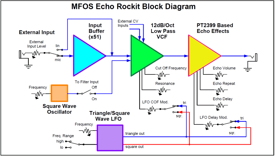
Block Diagram
Table of Contents
An Echo Rockit in Your Modular? - Possible But...
Table of Contents
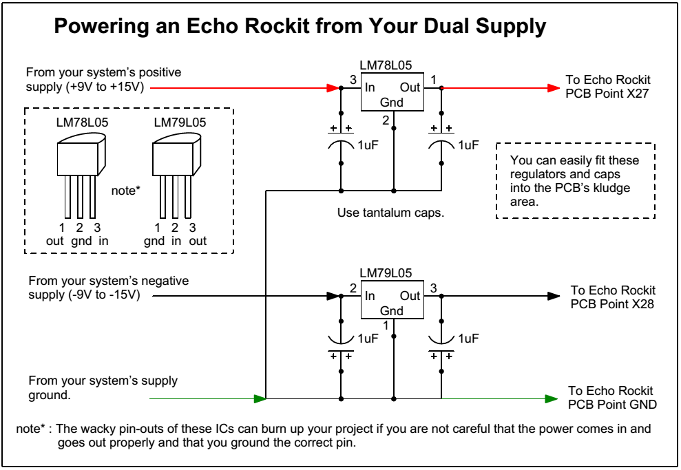
On a small bread-board, power an LM78L05 from your system's positive rail and an LM79L05 from your system's negative rail. Place 1uF tantalums at the input and output of each regulator. Remember to watch capacitor polarization. For the negative regulator the negative side of the caps go on the input and output of the negative regulator. Connect the +5V regulator's output to the Echo Rockit's positive battery connection (X27) and the -5V regulator's output to the Echo Rockit's negative battery connection (X28). Connect the power supply ground to the Echo Rockit's GND connection. Now the Echo Rockit will think it's powered from +10V and it's virtual ground will be at the same potential as your system's ground. The difference in operation from 9V to 10V is negligible. See the diagram below for more details.
Follow up... When I received the production PCBs I, of course, built one up to test. I tested it on the bench supply and on a battery and observed the 30mA current drain and played with it a bit to insure it was working fine. After that I installed the LM78L05 and LM79L05 regulators along with the 1uF tantalum capacitors on my test board in the kludge area and connected it to my modular supply. The Echo Rockit played nicely with my synth modules. This is a very versatile and fun project. Production boards are in house and for sale - click the cart icon located at the upper right to go to the catalog.
From the Anti-Smoke Department.
Table of Contents
Schematics
Schematic Page 1 Circuit Description
View as PDF Table of ContentsOn page one of the schematic we see the audio input buffer, the VCF voltage control mixer, the VCF and the PT2399 echo processor. The op amps used in the circuit are current conserving LM324 quad op amps (U1 and U5) in the 14 pin DIP package. The input is connected via J1 and dropped on 100K Input Level control pot R6. The wiper of R6 is connected to capacitor C6 which blocks DC and passes the AC portion of the level adjusted input signal to one of DPDT switch S1's common poles. With S1 up (Line position) the input signal is fed directly to the VCF's input at circuit point X1. With S1 in Mic position the signal is applied to a non-inverting buffer op amp with a gain of fifty one. Op amp U1-C has a 100K feedback resistor (R8) between its inverting input (pin 9) and its output (pin 8) and a 2K resistor from the inverting input to ground. Applying the non-inverting gain formula (Gain = (RFB/RGND) + 1) we see a gain of 51. This gain can be tailored if necessary. Making R8 higher in value will result in more gain and making R8 lower in value will result in less gain. Capacitor C8 (47pF) stabilizes U1-C to prevent oscillation due to its high gain. Resistor R3 (100K) keeps U1-C's non-inverting input biased to ground potential when S1 is in Line position and is high enough impedance not to form a significant high pass pole between C6 and itself when S1 is in Mic position.
Echo Rockit Schematic Page 1
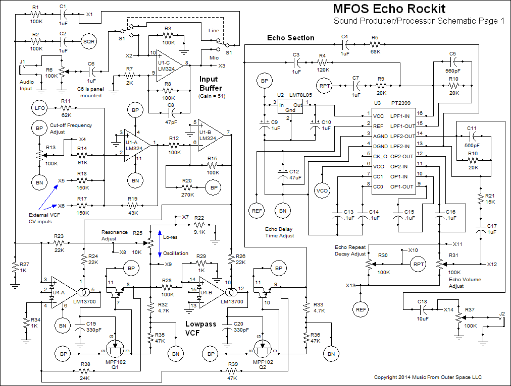
The VCF control voltage mixer is comprised of U1-A and U1-B and associated components. U1-A is used as an inverting DC voltage mixer for the VCF control voltage signals. You can manually adjust the cutoff frequency using R13, 100K Cut-off Frequency Adjust whose wiper is connected to 91K control voltage mixing resistor R14. LFO modulation is applied via 62K resistor R11. The values of the VCF's COF CV input resistors (R18 and R17 both 150K) can be tailored to your needs. Higher values will allow larger values of control voltage and lower values will allow the unit to be modulated by lower voltage signals. At the value shown in the schematic (150K) the expected external control voltage level is +/-5V. Higher control voltage won't damage anything but it also won't modulate the VCF any further than sub-audio to about 17KHz.
Notice that the internal LFO oscillates at a level of about +/-2V about the unit's virtual ground, thus the LFO modulation input is 62K which allows +/-2V to fully modulate the VCF. U1-A's 43K feedback resistor R19 gives us the gain reduction needed to bring the voltage swings in line with what the remaining circuitry needs. We re-invert the control signals using U1-B which supplies a gain of minus one (feedback (R15) and inverting input (R12) resistors are both 100K). Resistor R20 (270K) to BP applies an offset bias to the output of U1-B. Since we are applying a positive offset bias to the inverting input the op amp's output is biased negatively. We need the voltage to go from negative 4V to 0V in order to control the VCF properly. When the output of U1-B is at negative 4V very little current flows through resistors R24 and R26 into U4-A's bias inputs (pins 1 and 16 respectively) and the VCF's cut off frequency is very low. As the control voltage goes up the voltage at the output of U1-B goes from negative 4V towards ground thus more current flows into U4-A's bias inputs and the VCF's cut off frequency goes up. The LM13600 op amps act as voltage controlled resistors in this active filter application and low bias current makes them act like high value resistors (resulting in low cut off frequency) and high bias current makes them behave like low valued resistors (resulting in high cut off frequency).
The VCF is the same design as used in the MFOS Sound Lab Mark II and I was determined to get it to work on one 9V battery. Of course the incredibly cool LM13600 dual transconductance op amp (and all subs) is used to provide us with voltage control. Surprisingly few component values changed between those used for +/-12V and those used in this design running on +/-4.5V. Essentially the VCF is a two pole low pass filter with voltage controllable poles. The transconductance op amps in conjunction with their output capacitors (C19 and C20 both 330pF) act as voltage controlled integrators. The integrated audio signals seen on C19 and C20 are buffered by high impedance source followers (Q1 and Q2 both N-Channel JFET MPF102 or 2N5457). The input impedance of the LM13600's onboard darlington pairs is too low and causes distortions and phase inaccuracies that prevent the filter from achieving oscillation. That is why we buffer the current output onto the filter caps with the high impedance gates of the N Channel JFETs (Q1 and Q2). The output of the source followers is applied to the bases of the internal darlington pairs for buffering before driving additional circuitry. The 10K resonance adjust control R25 ranges between no resonance and sine wave oscillation at the extreme ends of the knob's rotation. The output of the filter (junction of U4-B pin 9 and R33) is applied to the input of the PT2399 echo processor chip via 1uF bipolar (non-polarized) DC blocking caps C3 and C4. The signal applied via C3 goes to the echo processor's input and the signal applied via C4 goes to the echo processor's output mixer and becomes the "original" signal.
Echo processing is provided by the amazing PT2399 chip which is covered in more detail in the ECHOFXXX voltage controlled echo module project. We power the PT2399 chip with a LM78L05 5V low power voltage regulator (U2). This chip can source 100mA at 5V but the PT2399 only needs about 15mA so this regulator works great. I tried a couple of zener/transistor based schemes and they used more current so the LM78L05 it is. We stabilize the input and output of the voltage regulator using 1uF tantalum capacitors. We add the 47uF cap called for in the data sheet to stabilize the PT2399's reference voltage (C12), the caps used in the modulator and demodulator (C14 and C13) and the caps for the low pass filters at U3 pins 9 and 10 (C15) and U3 pins 11 and 12 (C16).
Both U3's input summer op amp (U3 pins 15 and 16) and output summer op amp (U3 pins 13 and 14) have 20K feedback resistors in parallel with 560pF caps to provide some low pass filtering to the input and the output signals. This is to help reduce the noise associated with the sample edges in this one bit A to D scheme. The echo output signal is taken from U3 pin 12 and dropped on the resistive elements of R30 (100K Echo Repeat Adjust pot) and R31 (Echo Volume Adjust). We mix a portion of the echo output back into the input to achieve echo repeat via 100K Echo Repeat Adjust pot R30, C7 (1uF bipolar DC blocking cap), and resistor R9. The amount of signal fed back to the input determines how long the echoes continue to repeat. With R30 fully on the echo can cascade and build until it gets crazy. The Echo Volume Adjust (R31) allows you to add as little or as much echo to the output as you like.
The output of the VCF is applied to the input of U3 (pin 16) via 1uF bipolar capacitor C3 and 120K gain-reduction/mixer resistor R4. The signal is applied to the PT2399's onboard op amp LPF1-IN which is the gateway to the chip's sigma delta echo processor. The output of the Echo Rockit comes straight from the PT2399's on board op amp LPF2-OUT where it is applied via DC blocking cap C18 to the resistive element of Output Level pot R37. R37's wiper delivers the level adjusted output signal to the output jack (J2).
Schematic Page 2 Circuit Description
View as PDF Table of ContentsPage two of the schematic shows the LFO, the square wave oscillator, the voltage to current convertor used to modulate the Echo Rockit's echo delay time and the battery power supply with virtual ground.
The LFO uses two op amps (one as an integrator and one as a comparator) in conjunction to realize a triangle/square wave oscillator. Since we know that on power up a comparator will come up either saturated high or low we'll assume U5-B came up low (about -4V in relation to virtual ground). U5-B's output is connected to 1M LFO Rate potentiometer R51 which along with R54 (2K resistor) is wired as a variable voltage divider. As R51 is adjusted up and down, more or less of the output voltage of U5-B is presented at R51's wiper. The voltage at R51's wiper causes current to flow through R50 (62K resistor) to the inverting input of U5-A. Since out comparator's output is low the integrator's output will ramp up in voltage until it overcomes comparator U5-B's hysteresis (provided by R40, 390K resistor) and the voltage at the non-inverting input of U5-B goes above the voltage on the inverting input. At that point comparator U5-B's output shoots high (about +4V in relation to virtual ground) rapidly. Now the current through R50 is reversed and the integrator's output begins to ramp down until the voltage on the non-inverting input of U5-B is below the voltage on its inverting input and - whammo - the output of comparator U5-B shoots low again and the cycle repeats. This results in a triangular wave of about +/-2V oscillating about virtual ground appearing at the output of U5-A and a square wave output (+/-4V oscillating about virtual ground) at the output of U5-B. When pot R51 is adjusted toward R54 the voltage on R51's wiper is low resulting in less current flowing through R50 to the integrator's input and lower LFO frequency. When R51 is adjusted toward U5-B's output more voltage appears at the wiper resulting in more current flowing in and out of the integrator and higher LFO rate. Switch S2 allows a second capacitor (C21, 1uF bipolar cap) to be placed in parallel with C22. When you increase the plate area of the integrator's cap the range of the LFO's frequency is lowered. With S2 open (C21 not in the circuit) the LFO's rate ranges from about 2Hz. to 800 Hz. When S2 is switched in the LFO's rate ranges from about one cycle per 1.5 minutes to 6.7 Hz.
Echo Rockit Schematic Page 2
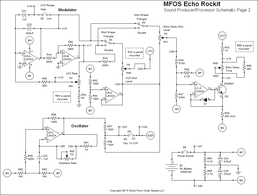
Switch S4, SPDT, selects either the triangle wave from U5-A's output or the square wave from U5-B's output (via attenuating resistor R44) to be routed to 1M VCF Mod Level pot R46. R46 is also wired as a variable voltage divider for the LFO's selected output. The level adjusted voltage on the wiper of R46 is used to modulate the cut off frequency of the units's VCF. Circuit point LFO is connected to R11 which adds the modulating LFO voltage to the other control voltages being mixed by U1-A (shown on page 1). Note that the "low" end of R46 is connected to the output of U5-D which is buffering a second virtual ground. I found that using this scheme quieted the unit's penchant to cause the main virtual ground to move up and down with the LFO's output resulting in unwanted filter cut off frequency modulation. This same virtual ground (output of U5-D) is used by the internal oscillator's output voltage divider (R58 connects to it) and the low side of the Echo Delay Mod control pot (R41).
Switch S3, SPDT, (Echo Delay Mod Shape) selects either the triangle wave from U5-A's output or the square wave from U5-B's output (via attenuating resistor R44) to be routed to 1M Echo Delay Mod Level pot R41. R41 is also wired as a variable voltage divider for the LFO's selected output. The level adjusted voltage on the wiper of R41 is fed to the voltage to current convertor used to modulate the echo delay time of the unit's PT2399 echo processor chip (U3 on page one). Resistors R5 (510K), R47 (240K) and R48 (4.7M) both attenuate and bias the selected modulation waveform's voltage which is presented to the non-inverting input of U1-D so that the output of U1-D drives the current sink transistor Q3 in the proper region to modulate the PT2399's voltage controlled clock.
Manual Echo Delay control R49 (100K) is paralleled with R66 (39K). The parallel resistor lowers R49's maximum resistance so that the echo delay clock rate does not get excessively low with resultant noise. If you would like the echo delay clock rate to be able to go really low - leave off R66. The VCO control pin of U3 (pin 6) is connected to series connected 1K resistor R42 and R49 (wired as a variable resistor), and the collector of Q3. With R41 turned all the way down Q3 is conducting so that R49 gives full adjustment to the Echo Delay Time. When R41 is turned up the voltage on the non-inverting input of U1-D causes Q3 to sink more or less current which raises and lowers, respectively, the rate of the PT2399's VCO resulting in modulation of it's echo delay. D1 clamps the output of U1-D to 600 mV to protect Q3's base from excessive voltage and current. The two controls (R41 Echo Delay Mod and R49 Echo Delay Time) work interactively to set the PT2399 VCO's frequency and modulation amount.
The unit's simple square wave oscillator used to excite the unit's VCF is comprised of one op amp with both positive and negative feedback. U5-C is dominated by it's function as a comparator. Again we can start to analyze the circuit knowing that the output of U5-C will come up either high or low on power up. We'll assume it came up high for our discussion. Notice that resistor R59 is connected to a third virtual ground at the junction of R62 and R63 (both 10K resistors). On power up capacitor C23 (.1uF) will be at ground but will immediately begin to charge toward the voltage on the output of U5-C (about +4V in relation to virtual ground) via series connected 1K resistor R61 and Oscillator Rate pot R60 (wired as a variable resistor). When the voltage on C23 charges to the point that the voltage on the inverting input of U5-C is higher than the voltage on U5-C's non-inverting input U5-C's output shoots low. Now capacitor C23 begins to discharge toward the voltage on U5-C's output (about -4V in relation to virtual ground) until it's voltage goes below the voltage on U5-C's non-inverting input and - whammo - the output of U5-C shoots high and the cycle continues resulting in square wave oscillation at the output of U5-C. Oscillator Rate pot R60 adjusts the rate of the internal oscillator between about 3 Hz. and 1.4 KHz. Resistors R57 and R58 attenuate the square wave output so that it does not overdrive the VCF. When S5 is closed the square wave is applied to the VCF's audio input via C2 (1uF bipolar) and 100K attenuating resistor R2.
The unit is powered by one nine volt battery and average current drain is about 30mA. Circuit point BP is the switched (via S6) positive terminal of the battery and circuit point BN is the battery's negative terminal. A virtual ground is created at 1/2 the battery voltage by resistors R64 and R65 (both 4.7K resistors) and stabilized by 470uF capacitors C24 and C25. This ground is used throughout the circuit.
The unit's front plate is connected to virtual ground. The battery's positive or negative terminals should NEVER come into contact with the unit's front plate. Attempting to switch the battery's negative terminal with a switching jack that is in contact with the virtual ground will short one half of the virtual ground and will not work.
PC Board Information
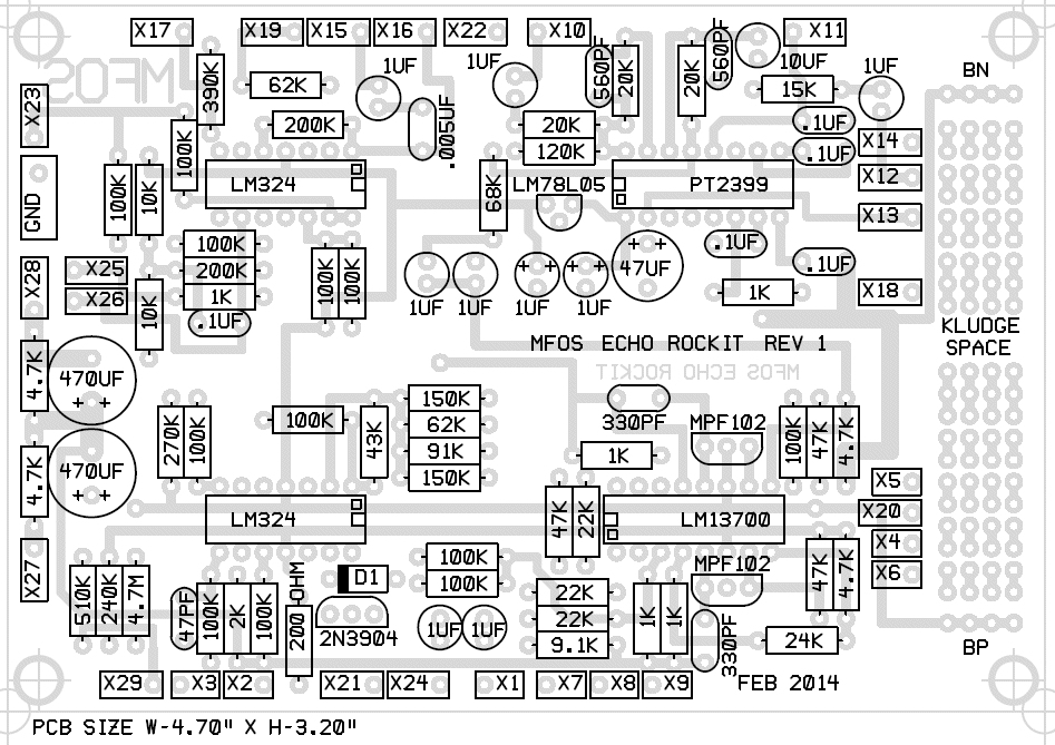
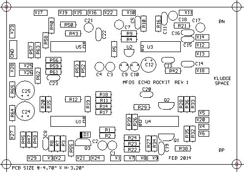
Table of ContentsParts Layout With Component Values
Print out this view to use when you are populating the PC board. Not having to continually refer between designators and the schematic will save you a lot of time.
C22's value can be .005uF or the more readily found .0047uF. Both work perfectly.
I actually increased the size of the board a bit to provide the proto kludge area. An 8 pin DIP can fit there as well as enough components to be dangerous. The BN and BP symbols indicate the switched battery terminals.
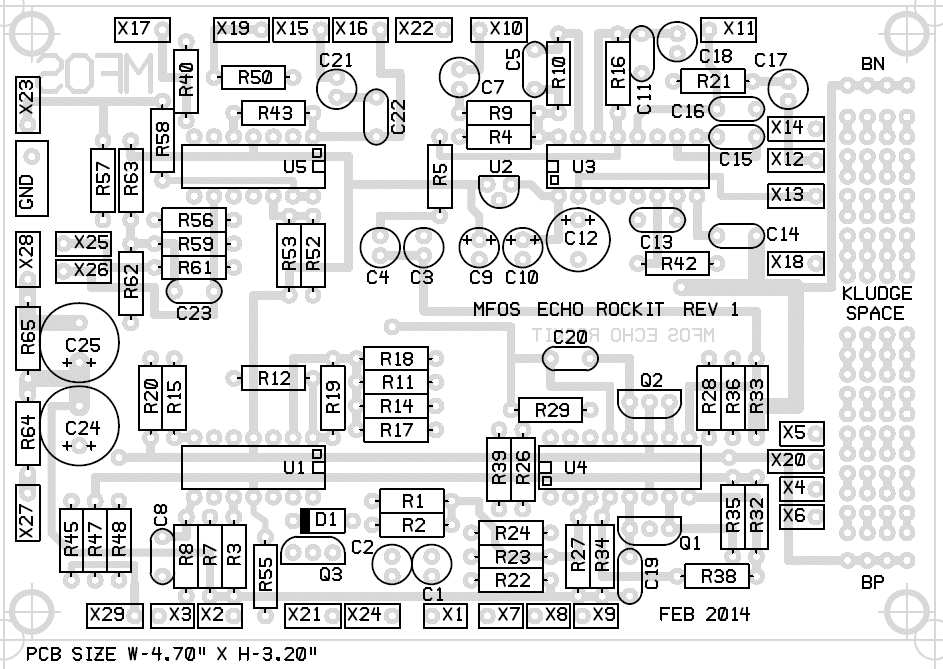
Parts Layout With Component Designators
When you are trouble shooting you'll need this view so that you can refer between the designators and the components shown in the schematic.
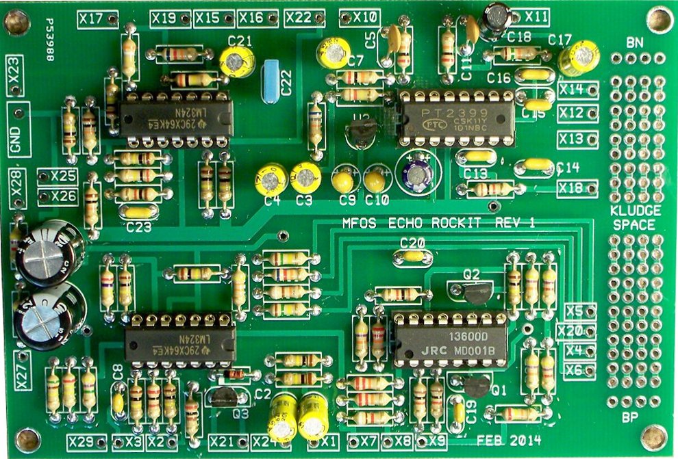
Populated PC Board
Here is a photo of the Echo Rockit PC board after populating it with the components.
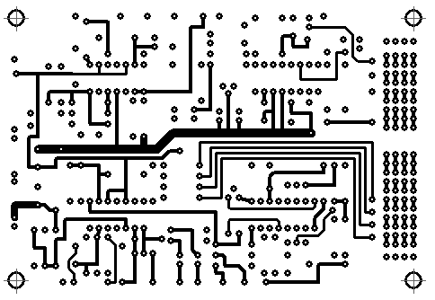
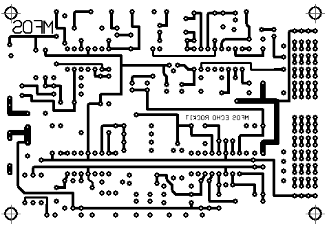
Top Copper
MFOS PCB Images are as viewed from the top of the PC Board. Keep that in mind when you are using the patterns with photo or copier processing.
Bottom Copper
MFOS PCB Images are as viewed from the top of the PC Board. Keep that in mind when you are using the patterns with photo or copier processing.
Silk Screen
MFOS PCB Images are as viewed from the top of the PC Board. Keep that in mind when you are using the patterns with photo or copier processing.
Kludging/Bending PCB Points of Interest
Table of ContentsThis view is as seen from the bottom of the PC board.
Here we see some points you may be interested in when kludging or bending the unit. For the two points that are inverting op amp inputs you should only connect to them via a resistor of 15K or higher to mix in a signal if desired. I suggest you keep impedances high everywhere you can if kludging to conserve current.

Front Panel Information
Table of Contents
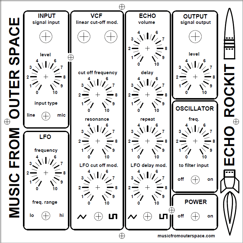
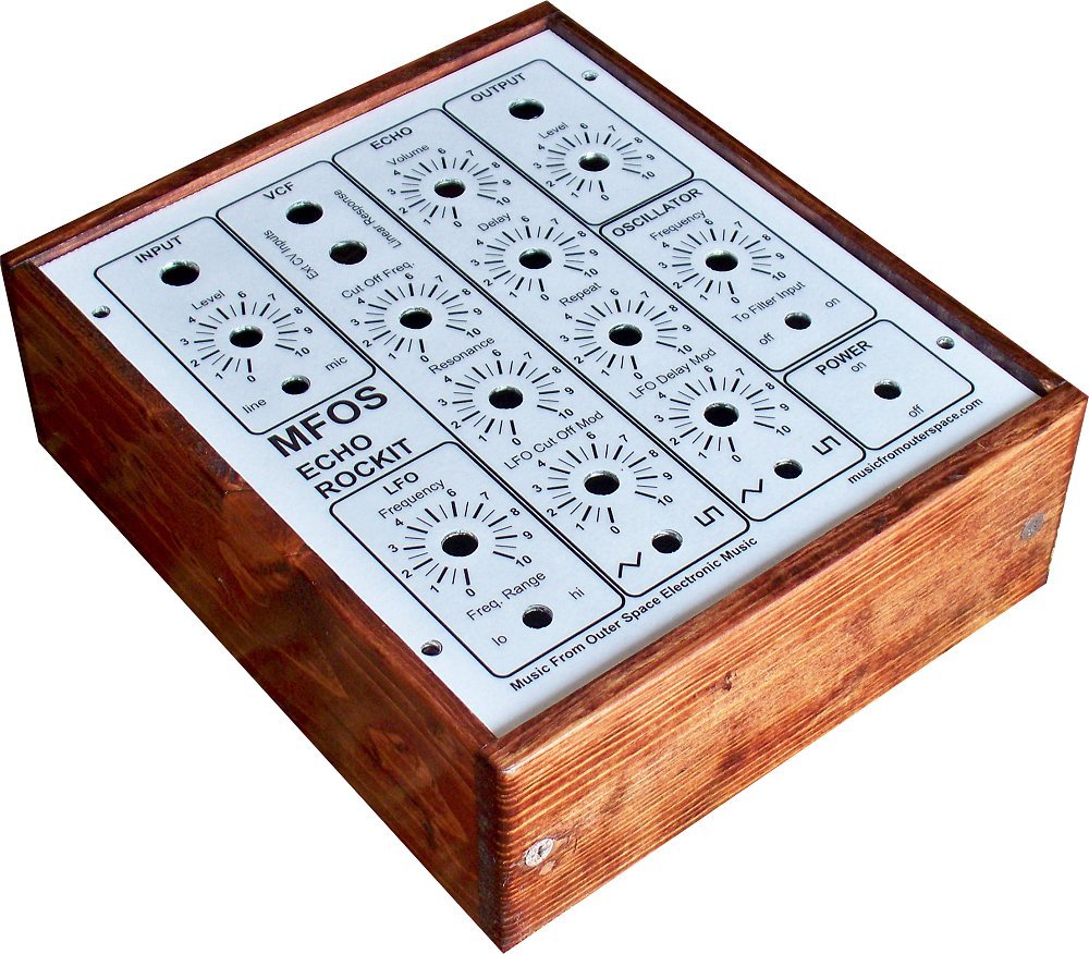
Suggested Front Panel Layout
View as PDFThe PDF should print out to scale if you decide to use this panel design for your project. The jack mounting holes should be drilled with a 3/8" bit, the mini-toggle switch mounting holes with a 1/4" bit, the potentiometer mounting holes with a 5/16" bit and the panel mounting holes with a 5/32" inch bit.
The unit's front plate is connected to virtual ground. The battery's positive or negative terminals should NEVER come into contact with the unit's front plate. Attempting to switch the battery's negative terminal with a switching jack that is in contact with the virtual ground will short one half of the virtual ground and will not work.
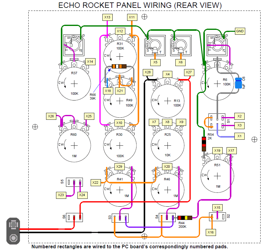
Suggested Front Panel Wiring Diagram
View as PDFAlways carefully review your wiring as this is where 90% of errors are made. Leaving off any connection will cause unexpected behavior and bugs. Don't turn your iron temperature up too high when soldering components with plastic parts or you may melt them.
Mounting the PC board on the MFOS plate
There are two holes on the front panel that line up with the holes on the PCB and can be used to mount the PCB. Mounting is accomplished using 1.25" long 6-32 machine screws, 6-32 machine nuts and nylon spacers or standoffs that stand the board off of the plate by at least 3/4". That way the board is well above the pot bodies. Mount the board with the components facing up away from the panel and panel components.
Echo Rockit Project Parts List
Table of Contents
Component Notes
All cap voltages should be 25V or more. All resistors are 1/4W 5% (1% will work fine). MFOS PC boards use dual inline IC packages. MFOS PC boards usually use 5mm (0.2") cap lead spacing unless it is obvious from the board's legend that it should be larger or smaller. I often specify axial leads for any caps mounted on the front panel but you can use radial as well by adding some wire to the leads. The potentiometers can be rated for 1/4W and all are linear taper. All components need to have leads. Be sure you are not buying surface mount parts. USE IC SOCKETS!
| Qty. | Description | Value | Designators |
|---|---|---|---|
| 1 | LM13700 Dual gm OpAmp | LM13700 | U4 |
| 2 | LM324 Quad Low Power Op Amp | LM324 | U1, U5 |
| 1 | LM78L05 5V Voltage Regulator | LM78L05 | U2 |
| 1 | PT2399 Echo Processor IC | PT2399 | U3 |
| 2 | MPF102 | MPF102 | Q1, Q2 |
| 1 | Transistor NPN 2N3904 | 2N3904 | Q3 |
| 1 | 1N914 Sw. Diode | VALUE | D1 |
| 1 | Potentiometer Linear taper | 10K | R25 |
| 4 | Potentiometer Linear taper | 1M | R41, R46, R51, R60 |
| 6 | Potentiometer Linear taper | 100K | R6, R13, R30, R31, R37, R49 |
| 1 | Resistor 1/4 Watt 5% | 390K | R40 |
| 4 | Resistor 1/4 Watt 5% | 4.7K | R32, R33, R64, R65 |
| 1 | Resistor 1/4 Watt 5% | 4.7M | R48 |
| 1 | Resistor 1/4 Watt 5% | 43K | R19 |
| 3 | Resistor 1/4 Watt 5% | 47K | R35, R36, R39 |
| 2 | Resistor 1/4 Watt 5% | 150K | R17, R18 |
| 1 | Resistor 1/4 Watt 5% | 510K | R45 |
| 1 | Resistor 1/4 Watt 5% | 68K | R5 |
| 1 | Resistor 1/4 Watt 5% | 9.1K | R22 |
| 1 | Resistor 1/4 Watt 5% | 91K | R14 |
| 2 | Resistor 1/4 Watt 5% | 62K | R11, R50 |
| 12 | Resistor 1/4 Watt 5% | 100K | R1, R2, R3, R8, R12, R15, R28, R52, R53, R56, R57, R58 |
| 2 | Resistor 1/4 Watt 5% | 10K | R62, R63 |
| 1 | Resistor 1/4 Watt 5% | 120K | R4 |
| 1 | Resistor 1/4 Watt 5% | 39K | R66 |
| 1 | Resistor 1/4 Watt 5% | 15K | R21 |
| 5 | Resistor 1/4 Watt 5% | 1K | R27, R29, R34, R42, R61 |
| 1 | Resistor 1/4 Watt 5% | 200 ohm | R55 |
| 3 | Resistor 1/4 Watt 5% | 200K | R43, R44, R59 |
| 3 | Resistor 1/4 Watt 5% | 20K | R9, R10, R16 |
| 3 | Resistor 1/4 Watt 5% | 22K | R23, R24, R26 |
| 1 | Resistor 1/4 Watt 5% | 240K | R47 |
| 1 | Resistor 1/4 Watt 5% | 24K | R38 |
| 1 | Resistor 1/4 Watt 5% | 270K | R20 |
| 2 | Resistor 1/4 Watt 5% | 2K | R7, R54 |
| 1 | Capacitor Aluminum Bipolar (non polarized) | 10uF | C18 |
| 8 | Capacitor Aluminum Bipolar (non polarized) | 1uF | C1, C2, C3, C4, C6, C7, C17, C21 |
| 1 | Capacitor Ceramic | .005uF or .0047uF | C22 |
| 5 | Capacitor Ceramic | .1uF | C13, C14, C15, C16, C23 |
| 1 | Capacitor Ceramic | 47pF | C8 |
| 2 | Capacitor Ceramic | 560pF | C5, C11 |
| 2 | Capacitor Ceramic | 330pF | C19, C20 |
| 2 | Capacitor Electrolytic | 470uF | C24, C25 |
| 1 | Capacitor Electrolytic | 47uF | C12 |
| 2 | Capacitor Tantalum Electrolytic | 1uF | C9, C10 |
| 1 | DPDT Switch | on-on (no middle position) | S1 |
| 2 | SPDT Switch | SPDT | S3, S4 |
| 3 | SPST (or SPDT) Switch | SPST | S2, S5, S6 |
| 4 | Jack (2 Conductor) | Mono Phone Jack | J1, J2, 2x CV Input Jacks |
| 1 | Battery | 9V Battery | B1 |
| 25ft. | 22 AWG Stranded | Stranded Wire | For all wiring. |
Echo Rockit Project Kit Notes
Table of ContentsEcho Rockit KIT PART LIST PDF - This is what comes in the kit.
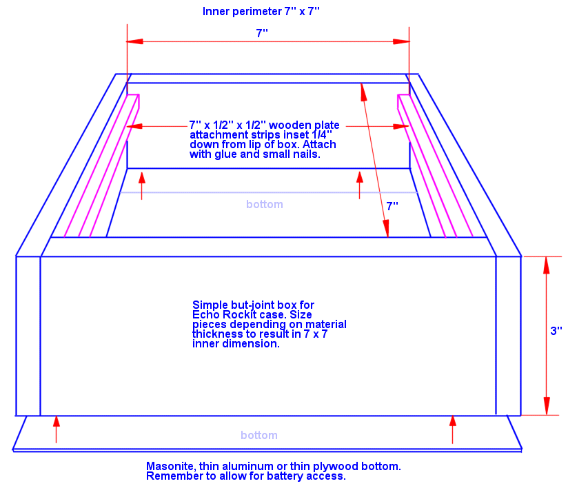
My Simple DIY Case
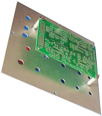
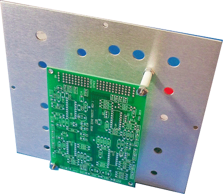
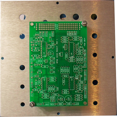
Although this case reflects the original panel size (more rectangular) the new plate is 7" x 7" x 1/16" thick. Remember to make the inner dimensions 7" x 7" to accommodate the plate. Many of the ideas shown still apply although the form factor is now square.
I had great plans to be able to recommend the BUD AC-405 for this project but the holes in the plate don't line up with the holes in the BUD box. A few choice expletives were uttered upon discovering this. I tried to follow the BUD drawings but I goofed plain and simple. You could modify the holes in the BUD box or drill new holes if you like to mount the plate on it.
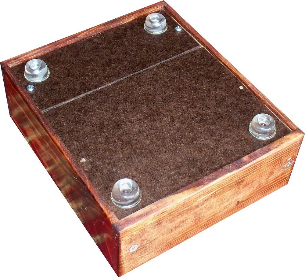
I made my case from pine and my faceplate from 1/16" thick aluminum. I covered the faceplate with a legend template made out of laminated paper. The case is very rudimentary and simply holds the PC board, battery, faceplate and the controls. I used a dado blade on my table saw to make the shelf to which the faceplate is attached with screws. The dimensions should accomodates the front panel you make and be deep enough for the PC board, controls and wiring. I used masonite (thin composite wood) for the bottom of the case and I split the bottom cover into two parts so that I can access the battery. The half containing the PC board is glued on but the battery access port is attached with screws for convenient removal. I got the nice stick-on rubber feet at All electronics. Click any image to see a larger view.
 |
 |
 |
 |
Making a Faceplate
I have published a YouTube that demonstrates how to make a nice looking faceplate by using the faceplate PDF I provide on the site.
YouTube of How To Make Synth Front Panels Part I
YouTube of How To Make Synth Front Panels Part II
Obtaining Parts
Kits and components for your MFOS projects can be found at Small Bear Electronics and SynthCube.
Resistor Color Chart For Resistors Used In This Project
The resistors should be carbon composition or carbon film. Use 1/4 watt resistors because 1/2 watt will be too big for the board. You can use 1/4W 1% metal film resistors for any or all resistors if you want to. Metal film resistors have less temperature drift than carbon composition or film resistors but for this application carbon film or composition work perfectly.
Capacitor Markings For Caps Used In This Project
All capacitors should have a minimum 16V rating. There really is no maximum voltage rating but capacitors get larger as the voltage rating goes higher. I suspect that electrolytics rated at 25V, 35V or even 50V will still be small enough to fit the board. For ceramics the voltage rating can be much higher. The voltage rating is NOT CRITICAL except that ALL CAPS SHOULD BE AT A MINIMUM rated for 16V. The lead spacing for most caps on the boards from MFOS is 0.2" (5mm) but you can always make leads with smaller (or larger) lead spacing fit so that is not a big deal.
Capacitor manufacturers have a variety of ways of marking the values on the components. When a cap is not plainly marked as .1uF (spoken as "point one microfarad") it will be marked in picofarad style. It will be marked like this: 104 which means 10 followed by 4 zeros picofarads. or 100,000 picofarads (or .1uF)
When capacitor values fall into a certain negative power of 10 they are given prefix names. Typically micro and pico with some folks occasionally using nano. So if a cap has the value of .0001 Farad we say it is 100 microfarads (or uF).
| milli | micro | nano | pico | |
| . | 000 | 000 | 000 | 000 |
If a cap has the value of .0000001 Farads we say it is .1uF (point one micro farad) but you could also say 100,000 pico farads, or 100 nano farads and be correct. You can see how the marking "104" takes up less space and space is at a premium on small parts.
So... with all that said .01 uF will be marked as 103 (10,000 pF) and 330 pico farads will be marked as 331. The next time you look at a cap I hope you are better able to tell it's value.
More examples (from this project)
Switches
The switches in this circuit are switching very low currents so they do not need high voltage or current ratings. Typical miniature toggle switch ratings are 1 to 5 amps at 115VAC which is way more than they will ever see in this circuit but that's what they make. Buy the cheapest switches you can because they will work fine. Of course if your last name happens to be Gates, Buffett, or Ellison you can buy gold plated toggle switches if you like since as long as they are the correct type (SPST (SPDT will also work as SPST)) they will all work.
More information
- Tell me something about switches?
- Reading Resistor Values
- What is a capacitor and what do the numbers on the capacitor mean?
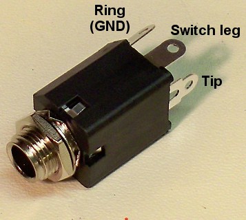
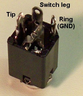
1/4" Phone Jack
This Amphenol jack (Amphenol Part# ACJM-MVS-2S) is currently shipping in kits. It is always best to ring out whatever jack you use with your multi-meter to make sure of which terminal is which. Don't let the normally closed switch fool you as to which terminal is the tip. Stick a piece of paper between the switch leg and the jack to open the connection while ringing out the jack.
 |
 |
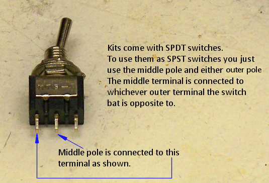
Kits come with SPDT switches which work perfectly as SPST
I send all Single Pole Double Throw Switches in kits because they also serve perfectly as SPST switches. As you can see in this image the switch has three terminals. The middle terminal is common and is connected to either of the outer terminals depending on the position of the switch bat. The terminal that is opposite of the way the switch bat leans is the terminal in contact with the middle terminal. Either outer terminal can be used.
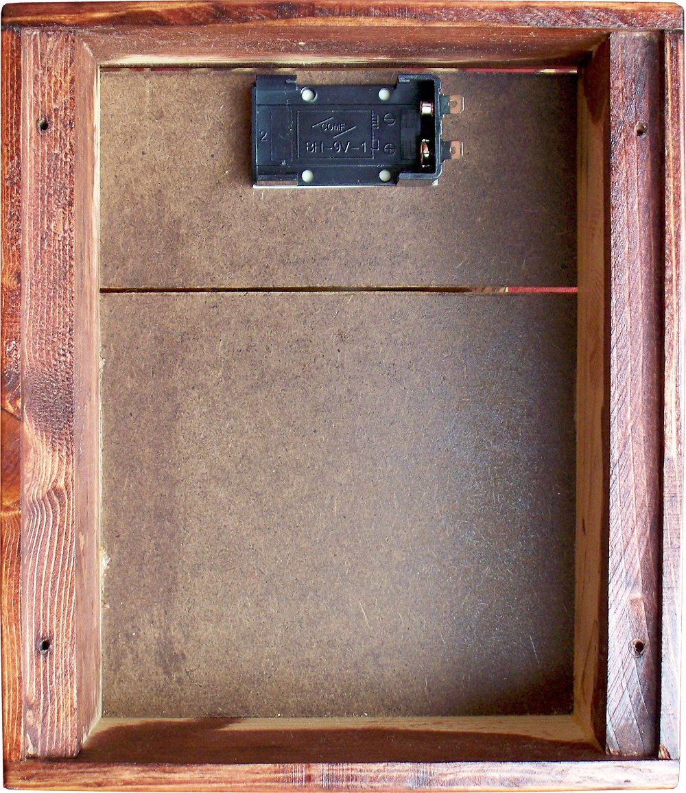
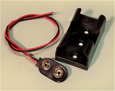
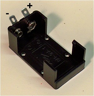
Battery Holder and Battery Snap
Some kits come with a battery holder and separate battery snap with wires while others come with a battery holder with an integrated battery snap and terminals to which you must solder wires to connect to the circuit board and/or front panel. The battery holder with the integrated battery snap is clearly marked as to which terminal is positive and which is negative. I suggest that you use two different colored wires so as not to confuse which is positive and which is negative (red and black would be a good choice). Mount either battery holder using small flat head screws (#6 flat head philips screws work well).
 |
 |
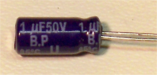
Bipolar or Non-Polarized Caps
Don't confuse your caps. The bipolar (or non-polarized) aluminum caps look kind of like electrolytic caps except they have no + or - markings. Instead the cap is marked B.P.
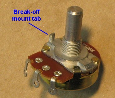
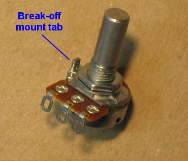
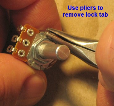
How To Remove Break-off Lock Tabs From Your Potentiometers
| If your pots have little tabs on them you will need to remove them so that you can mount them to your faceplate. It is really easy to do. Carefully snap off the little tab near the pot body and voila it's done. Some kits come with larger pots and some kits come with smaller pots. The smaller pots are at times more expensive than the larger pots. They're all good quality pots and they all work the same way. | |
Regular Sized Pots |
Smaller Sized Pots |
|---|---|
| This is the break-off lock tab which can be used to keep the pot from turning when you turn the pot shaft but tightening the mounting nut works just fine. If you have the wherewithal to drill little holes for these pesky things... be my guest. If not... read on. | |
 |
 |
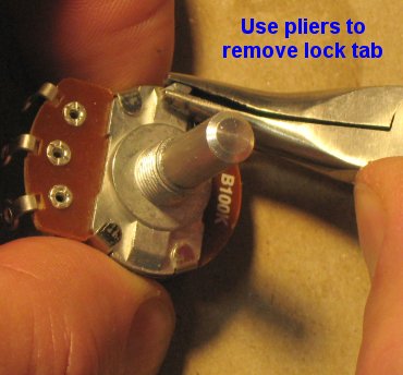
| Using pliers, grasp the tab as low on it as you can and then gently twist the pliers outward. I told you it was easy. | |
 |
 |
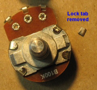
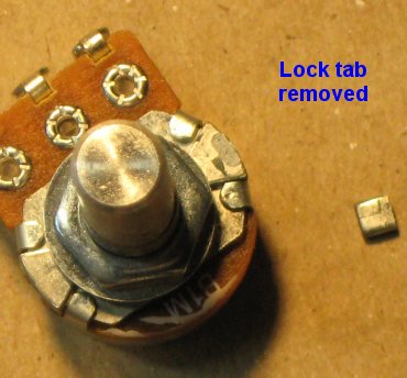
| The little broken off tabs look like this. Now you can mount your pot without the little tab getting in the way. | |
 |
 |