Ray Wilson authored this content while he was actively running MFOS as the founder and resident genius.
We retain the content because it reflects a valuable point of view representing that time and place.
Article by Ray Wilson
Features
IntroductionA great assortment of functions in one module. Two 3 input DC voltage mixers with normal and inverted output, a linear lag processor, an RC lag processor and a LED voltage level meter. The voltage meter looks cool and lets you have a graphical idea of where that voltage level you like to use to modulate your filter or vca is so that later repeating it will be easier.Although simple in nature the voltmeter is useful and has several input ranges (+/-1V, +/-5V and +/-10V). Whereas an analog or even a digital meter takes time to find the level this circuit lights the LED immediately giving you a rough idea of the voltage level you're looking at even when it is changing rapidly. The DC mixers let you mix LFO outputs or any voltage sources. The lag processors both give plenty of range to go from almost immediate voltage following to delays lasting many seconds before the output voltage arrives at the level fed into the input. |
|

While trouble shooting an issue I discovered a problem related to reverse bias on tantalum capacitors. When tantalum caps are exposed to reverse bias they develop leakage leading to eventual failure. A few circuits use tantalums where non-polarized aluminum caps would be a better choice. I have looked over all of the MFOS circuits and identified a small number of circuits where this may result in a problem. This circuit is one of the affected designs. I have not had any reports from the field regarding this and discovered it when my ULTIMATE's sample and hold clock started acting oddly.
If you start to see the log lag processor become sluggish even at low settings of the pot I recommend that you change C22 (2.2uF Tantalum Capacitor) to a 2.2uF non-polarized aluminum capacitor. As the lag capacitor in the log-lag circuit this capacitor can be exposed to negative voltage if it is applied to the input. The part list has been updated to reflect this.
THE PC BOARD LEGEND FOR C22 HAS A POLARITY MARKING. IGNORE IT WHEN INSTALLING THE NEW NON-POLARIZED CAP
Multi-Function Module Schematic Page 1 (LED Volt Meter) PDF
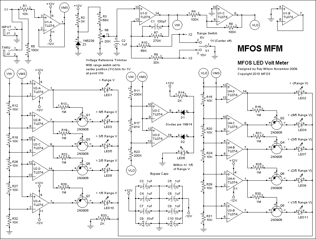
Page one of the schematic contains the voltage meter. Starting at the top of the schematic we see the voltage input buffer (U1-A) which is used as a unity gain voltage follower. We also find the voltage range selection circuitry (U1-D and U1-C and associated components). The 1N5239 9.1V zener is used for range selection reference generation. 9.1V is generated at the junction of current limiter R2 and the cathode of Z1. This is fed to the resistor divider R3 and R6. R6 must be adjusted so that there is 1.00V on the output of U1-D (pin 14) when S1 is in the center position. Unity gain followers have the gain formula (1 + R-feedback/R-Gainset). When switch S1 is in the center position there is no R-Gainset in the circuit and the follower gives a gain of 1. With R9 in the circuit (S1 set to the 10V range setting) the gain goes to 10 (1 + 270K/30K) and with R10 in the circuit the gain is very close to 5 (actually 4.97) which is more than close enough for this circuit. Notice that the output of U1-D is fed into the input of unity gain inverter U1-C. U1-C's output will always be U1-D's output multiplied by negative one. When U1-D's output is 1V, U1-C's output is -1V. When U1-D's output is 5V, U1-C's output is -5V. When U1-D's output is 10V, U1-C's output is -10V. Thus S1 sets the voltage levels that are fed to both VHI and VLO between +/-10V, +/-1V and +/-5V.
The heart of the circuit is the group of comparators at the bottom of page 1 of the schematic. Notice that the VHI circuit point is the output of U1-D and the VLO circuit point is the output of U1-C. VHI is dropped on a series of 10K resistors (R12, R18, R26, R27, R32) which act as a voltage divider. So when VHI is 10V (S1 set to 10V range) there will be 10V at pin 2 of U2-A, 8V at pin 6 of U2-B, 6V at pin 9 of U2-C, 4V at pin 13 of U2-D, and 2V at pin 2 of U3-A. In general the resistor dividers will see to it that 1/5, 2/5, 3/5, 4/5, and 5/5 of VHI and VLO will be used as the comparator threshold settings no matter what range you are set for. These levels are fed to the inverting inputs of the respective op amps which are used as comparators. They comprise the reference input voltages to the comparators. In this configuration the output of each of these op-amps will be low (-11V) or high (+11V) depending on the voltage level fed to each ones non-inverting input.
Circuit point VMS (V-Measured), the output of op amp U1-A unity gain follower is applied to all of the the non-inverting inputs of these op amps (used as comparators) U2-A, U2-B, U2-C, U2-D, and U3-A. When VMS is at ground all of the outputs of U2-A, U2-B, U2-C, U2-D, and U3-A are low. If VMS goes above 2V the output of U3-A goes high and current can flow through Q7 (PNP transistor), LED10 and R33. Q7 conducts the current from U3-A's output through the LED and R33 because U2-D's output is low (-11V) which keeps Q7 (PNP transistor) turned on. If the voltage on VMS goes above 4V then the output of U2-D goes high. U2-D's output being high now turns on LED8 via current through Q8 and R33 but U2-D's output also turns off Q7 thus LED10 goes off. If the voltage on VMS goes above 6V guess what happens... OK, now LED5 glows because of current through Q3 but both Q5 and Q7 are turned off because of the high levels on the outputs of U2-C and U2D. So the basic idea is that as the voltage goes higher the next higher comparator will go high and thus the LEDs below that level are turned off. This configuration ensures that only one LED is on at a time and thus conserves current and in my book looks cooler.
The right side of schematic page 1 shows the circuitry used to meaure the negative voltage. As you can see the principle is the same however the inverting and non-inverting inputs of the comparators are switched and the references generated across the 10K resistors in series (R15, R20, R24, R29, and R31) are applied to the non-inverting inputs and that VMS is applied to the inverting inputs. Now the voltage level on VMS has to go below the reference voltage in order for the outputs of these comparators to go high. Remember that when VHI measures 10V volts that VLO measures -10V. What this means is that there is -10V at pin 12 of U4-D -8V at pin 10 of U4-C -6V at pin 5 of U4-B -4V at pin 3 of U4-A -2V at pin 5 of U3-B. So if VMS goes below -2V then the output of U3-B goes high (+11V) and current can flow through Q8, LED11 and R33 thus lighting LED11. If the voltage on VMS goes below -4V then U4-A's output goes high, turning on LED9 and turning off Q8 and in turn LED11. You can see that as the voltage goes lower the comparators continue to go high in turn illuminating their respective LED and turning off the preceding LEDs by turning off the preceding LED's control transistor.
LED6 is the "near ground" indicator and it lights if the voltage on VMS is between about +18.5% and -18.5% of the range setting. U3-C and U3-D comprise a window comparator. In order for LED8 to light, both U3-C and U3-D outputs must be high. If either output is low LED6 is robbed of current because either diode D1 or D2 is forward biased and sinking the current through R14 to -11V. When the voltage on VMS is between the two reference voltages applied to U3-C pin 10 and U3-D pin 13 then both comparator outputs are high and LED6 can light because current through R14 is not sucked into either D1 or D2.
Multi-Function Module Schematic Page 2 (Voltage Mixers) PDF
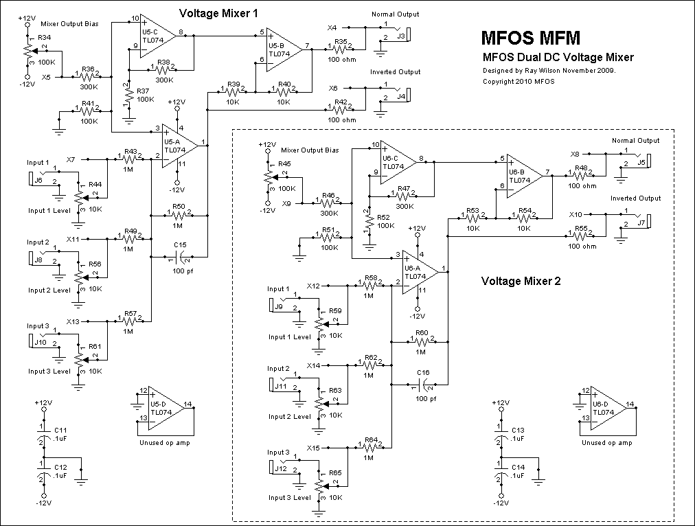
Page 2 shows the Voltage Mixers. I will only describe the operation of the one closest to the top of the page. The other circuit functions identically.
U5-A is the main voltage summer. The 10K level pots (R44,R56, and R61) feed the 1M input summing resistors (R43, R49, and R57) respectively. U5-A's feedback resistor is also 1M and thus it has a gain of one. The output of U5-A is fed to both the inverted voltage out jack and to the input of unity inverter U5-B which inverts the signal fed into it's inverting input and supplies it to the non-inverted outpus jack. Two inversions make a non-inversion just like -1 * -1 = 1. The bias control R34 applies between -12V and +12V to the top of the resistor divider made up of R36 (300K) and R41 (100K). Thus between +3V and -3V is applied to the non-inverting inputs of U5-C and U5-A as the bias knob is rotated from end to end. The DC offset applied to the non-inverting input of U5-A sees a gain of 2 because the formula for non-inverting gain is (1 + R-feedback/R-input) thus as the bias knob is adjusted the output of U5-A swings between -6V and +6V. Thus any signal at the output of U5-A can be offset by between -6V and +6V. Notice that buffer U5-C applies a gain of 4 to the DC level applied to it's non-inverting output. This is necessary so that the offset voltage applied to U5-B's non-inverting input is twice that applied to it's inverting input via U5-A's output. If the same bias was applied to U5-B's non-inverting input as is applied to U5-A's non-inverting input the net effect would be that U5-B would not reflect the desired DC offset but would remain at it's initial DC offset. This is because of common mode rejection. The same DC level applied to both the inverting and non-inverting inputs of an op-amp will result in an output of 0. Since we apply twice the DC offset to U5-B's non-inverting input we get the desired result. Both outputs move simultaneously up or down when we adjust the bias control. For example when we set the bias pot to have 1V of offset on the output of U5-A we will have 2V at the non-inverting input of U5-B. Since this is a difference of 1V, U5-B's output will have a DC offset of 1V, just what we want.
Multi-Function Module Schematic Page 3 (Lag Processors) PDF
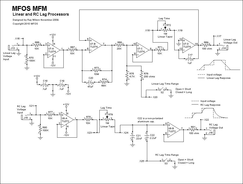
Page three of the schematic shows the two lag processors. The one at the top of the page provides a linear ramp between changes in voltage and the one at the bottom provides an RC curve between changes in voltage.
U7-A provides buffering for the voltage applied to the linear lag processor. U7-A's output is fed input U7-B's inverting input. U7-B provides a very high gain block which is used to detect the difference between the output of the integrator made up of U7-D and the input voltage. When the voltage on the input of the linear lag processor is higher than the voltage at the output of the integrator (U7-D) the output of U7-B is basically pegged at the lowest possible output voltage of U7-B about -11V (when using +/-12V). U7-B's output is fed to the top of a voltage divider made up of R68 and R75 (consider that S2 is open). The voltage divider and op-amp U7-C are used to lower the voltage and thus the current that is fed via series combination of R71 and lag adjust pot R72 to the input of integrator U7-D (and cap C17). In this situation (input voltage higher than integrator output) the low level fed to the integrator causes it to ramp up (at the rate determined by both the Short/Long switch selection and adjustment of R72). The integrator continues to ramp up until the voltage on the non-inverting input of U7-B equals the voltage on it's inverting input. At that point the op amp's output goes to 0 (remember common mode rejection). This zero (or ground) level is reflected at the output of follower U7-C and thus at the inverting input of U7-D. Since now both inputs are at ground the voltage on the output of the integrator is held since no current needs to flow in or out of U7-D's pin 13. The output just stays where it's at so as not to disturb the delicate balance on it's inputs. However if the input goes lower than the voltage on the output of the integrator the output of U7-B goes as high as it can (about 11V on +/-12V system) and drives the integrator down until the inputs balance again at which time the integrator's output again "holds". C20 and R74 in the feedback loop of U7-B minimize the ringing on the output of U7-B during transitions between either voltage extreme and ground and stabilize the op amp to avoid run away oscillation. When S2 is closed the 200 ohm resistor is put in parallel with the divider resistor R75 thus lowering the voltage level available to provide current to the integrator. You can get some VERY long lag times but the circuit follows the input very faithfully and eventually arrives at the input voltage plus or minus a millivolt or two.
The bottom of schematic page 3 contains the simple RC lag processor which is essentially an input voltage follower, a 1M pot, a selectable slew cap and another follower. C22 was formerly a 2.2uF tantalum cap but I have since replaced it with a 2.2uF non-polarized aluminum cap type because the cap can be exposed to reverse polarity if negative voltage is applied to the log-lag processor input. A nice low leakage film type cap (polypropylene for example) for C21 is also a good idea.
| Approx. Current Consumption | |
| +12V | 60mA |
| -12V | 60mA |
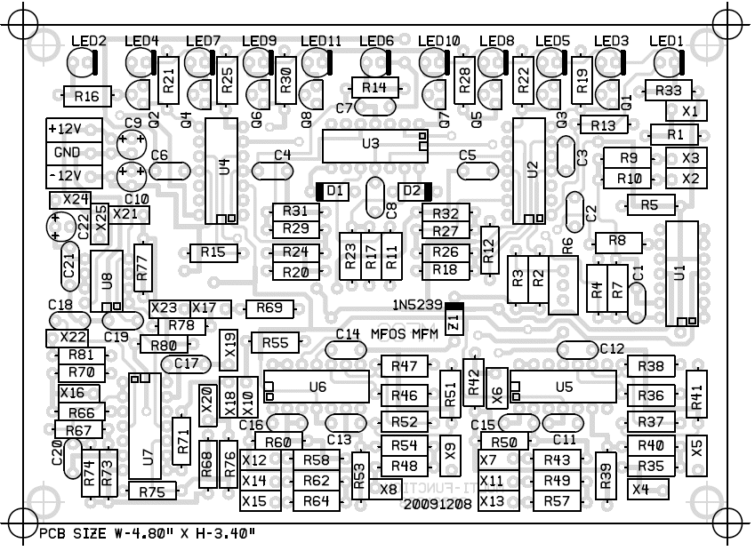
Multi-Function Module PCB Component Values (Parts Side Shown) PDF
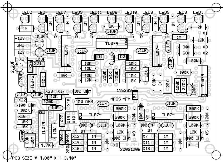
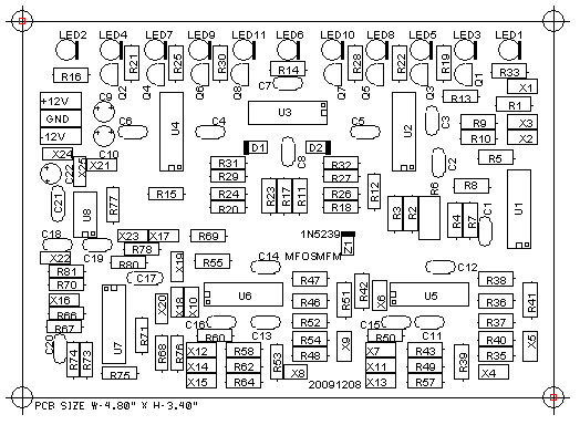
Multi-Function Module PCB Component Designators (Parts Side Shown) PDF
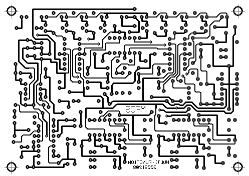
Multi-Function Module PCB Bottom Copper (Parts Side Shown)
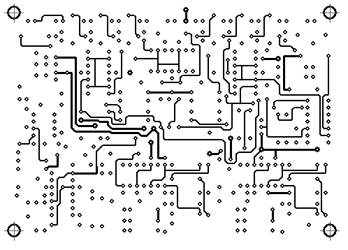
Multi-Function Module PCB Top Copper(Parts Side Shown)
Multi-Function Module PCB Top Silk Screen
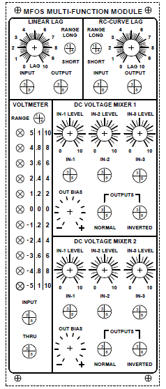
Multi-Function Module Front Panel
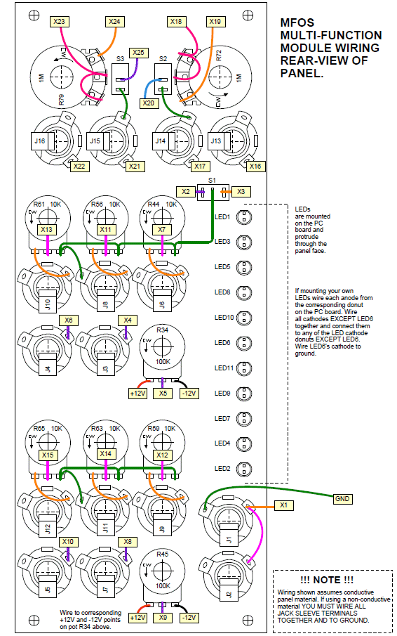
This panel is just a convenient way to show the controls included in the module and how to wire the unit. You will probably want to design your own. I used the side mounted LEDs in my panels and fashioned the panel and the mounting brackets to accomodate them but you can run wires from the board to the LEDs if you want to. Follow the schematic carefully to see how to wire up the anodes and cathodes of the LEDs. The RED led cathodes can all be wired together and then only one wire run to the board for them. The anodes must be wired separately. Remember that the "near ground" green LED needs to be wired separately.
| Size 4" x 10" | Size 3.5" x 8.75" |
 |
 |
Multi-Function Module DOTCOM Format Front Panel PDF
This cool panel was laid out by diyer Marv Kaye for his dot-com format synth. I suggest that you observe the wiring of the original panel and make a diagram to follow for the changes related to this panel if you decide to use it. You may need a graphics program to scale the image to proper size.
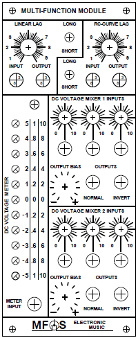
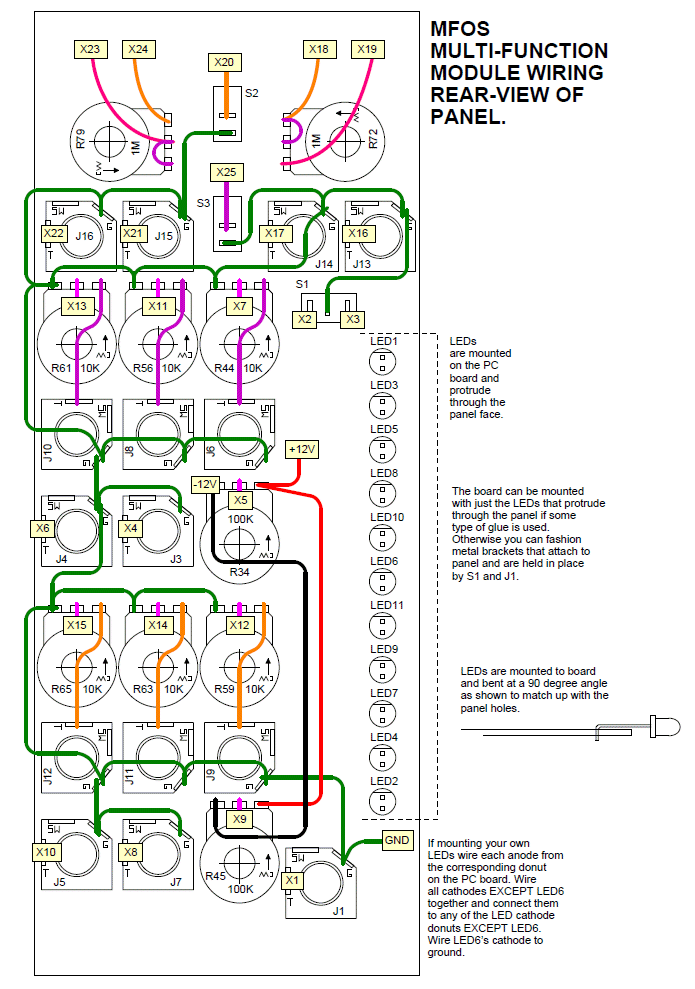
Multi-Function Module 4" x 10" Front Panel and Wiring Rear View PDF
This panel is just a convenient way to show the controls included in the module and how to wire the unit. You will probably want to design your own. Remember that this is the rear view of the panel and thus the controls are mirrored from the panel layout.
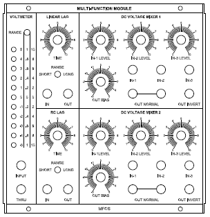
Multi-Function Module 3.5" x 8.75" Front Panel and Wiring Rear View PDF
This panel is just a convenient way to show the controls included in the module and how to wire the unit. You will probably want to design your own. Remember that this is the rear view of the panel and thus the controls are mirrored from the panel layout.
Multi-Function Module Project Parts List
| Qty. | Description | Value | Designators |
|---|---|---|---|
| 1 | TL072 Dual Op Amp | TL072 | U8 |
| 7 | TL074 Quad Op Amp | TL074 | U1, U2, U3, U4, U5, U6, U7 |
| 8 | Transistor PNP 2N3906 | 2N3906 | Q1, Q2, Q3, Q4, Q5, Q6, Q7, Q8 |
| 2 | Diode 1N914 | 1N914 or 1N4148 | D1, D2 |
| 1 | Diode Zener 9.1V 1N5239 or BZX55B9V1-TR | 1N5239 or BZX55B9V1-TR | Z1 |
| 1 | GREEN LED | LED | LED6 |
| 10 | RED LED | LED | LED1, LED3, LED5, LED8, LED2, LED4, LED7, LED9, LED11, LED10 |
| 2 | Linear Potentiometer | 100K | R34, R45 |
| 6 | Linear Potentiometer | 10K | R44, R56, R59, R61, R63, R65 |
| 2 | Linear Potentiometer | 1M | R72, R79 |
| 1 | Potentiometer Trimmer | 20K | R6 |
| 4 | Resistor 1/4 Watt 5% Carbon Film | 300K | R36, R38, R46, R47 |
| 1 | Resistor 1/4 Watt 5% Carbon Film | 30K | R9 |
| 1 | Resistor 1/4 Watt 5% Carbon Film | 3K | R2 |
| 1 | Resistor 1/4 Watt 5% Carbon Film | 4.7K | R75 |
| 3 | Resistor 1/4 Watt 5% Carbon Film | 68K | R3, R10, R74 |
| 1 | Resistor 1/4 Watt 5% Carbon Film | 91K | R17 |
| 6 | Resistor 1/4 Watt 5% Carbon Film | 100 ohm | R35, R42, R48, R55, R69, R81 |
| 9 | Resistor 1/4 Watt 5% Carbon Film | 100K | R4, R5, R8, R37, R41, R51, R52, R70, R80 |
| 20 | Resistor 1/4 Watt 5% Carbon Film | 10K | R1, R12, R15, R18, R20, R24, R26, R27, R29, R31, R32, R39, R40, R53, R54, R66, R67, R71, R77, R78 |
| 1 | Resistor 1/4 Watt 5% Carbon Film | 10M | R73 |
| 16 | Resistor 1/4 Watt 5% Carbon Film | 1M | R13, R16, R19, R21, R22, R25, R28, R30, R43, R49, R50, R57, R58, R60, R62, R64 |
| 1 | Resistor 1/4 Watt 5% Carbon Film | 200 ohms | R76 |
| 2 | Resistor 1/4 Watt 5% Carbon Film | 200K | R11, R23 |
| 1 | Resistor 1/4 Watt 5% Carbon Film | 20K | R68 |
| 1 | Resistor 1/4 Watt 5% Carbon Film | 270K | R7 |
| 2 | Resistor 1/4 Watt 5% Carbon Film | 2K | R14, R33 |
| 1 | Capacitor Ceramic | .22uF | C21 |
| 3 | Capacitor Ceramic | 100pF | C1, C15, C16 |
| 1 | Capacitor Ceramic | 1uF | C17 |
| 1 | Capacitor Ceramic | 47pF | C20 |
| 13 | Capacitor Ceramic | .1uF | C2, C3, C4, C5, C6, C7, C8, C11, C12, C13, C14, C18, C19 |
| 2 | Capacitor Electrolytic | 10uF | C9, C10 |
| 1 | Capacitor Non-Polarized Aluminum | 2.2uF | C22 |
| 1 | Switch SPDT (Center Off) | SPDT | S1 |
| 2 | Switch SPST | SPST | S2, S3 |
| 16 | Jack 1/4" 2 Terminal | Jack 1/4" 2 Terminal | J1, J2, J3, J4, J5, J6, J7, J8, J9, J10, J11, J12, J13, J14, J15, J16 |
Miscellaneous
- 1/16" Thick aluminum plate for mounting the pots and switches.
- Unit is typically mounted in a synth case with other synth modules.
- Assorted hardware 1" 6-32 nuts and bolts, 1/2" #8 wood screws, etc
- Knobs for potentiometers, wire and solder.
- Digital Volt Meter and a Signal Tracer or oscilloscope for testing.