Ray Wilson authored this content while he was actively running MFOS as the founder and resident genius.
We retain the content because it reflects a valuable point of view representing that time and place.
Article by Ray Wilson
Features
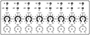
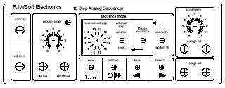
- 4 to 16 steps with coarse and fine tune adjustment.
- Modes: Forward-Reset, Forward-Reverse, Forward-Stop and Random
- Gate startable.
- Internal or Externally clocked.
- Gate switch at each step.
- Random mode and switched gates provide random gate capability.
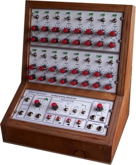
IntroductionThe main idea of a sequencer is to provide an automatic means of sequentially stepping through a series of adjustable voltages to drive a VCO (or any other voltage controlled device). Additionally, gate and trigger signals are generated at the moment the output of the circuit steps to a new voltage. Typically you use a sequencer to control the frequency of an oscillator (or several oscillators) to produce repeating tonal patterns, or arpeggios, which are further enhanced by filtering, modulation, addition of keyboard voltage etc. Sequencers are often used in electronic music production. This sequencer can produce a 4 to 16 note sequence. Additionally, this sequencer provides forward only, forward and back, and the unique ability for random sequencing. The gate/trigger can be included or not at each step (via a switch) and each step has coarse and fine voltage adjustment. Two circuit boards are required for this sequencer (unless you design your own) and I am offering both of them for sale. The digital board drives the sequencer and the analog board switches the control voltage from each set of coarse and fine pots to the output. You can start and stop the sequencer, reset it and step forward and/or backward to set up or manually walk through a sequence.
Yes, this works on +/-15 volts too. |
|
|
|
Cheers and Good Building, Ray |
||
MP3 SamplesReverse At Step Demo Reset At Step Demo Stop At Step and External Start Demo Gate Switch Demo (Gate switch setting are changed throughout) Dry Random Demo Wet Random Demo with two ocscillators Cool Sequence Demo |
||
Table of Contents |
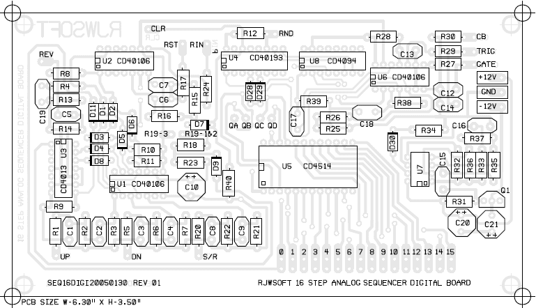
16 Step Analog Sequencer Digital Board Page 1 Click for PDF
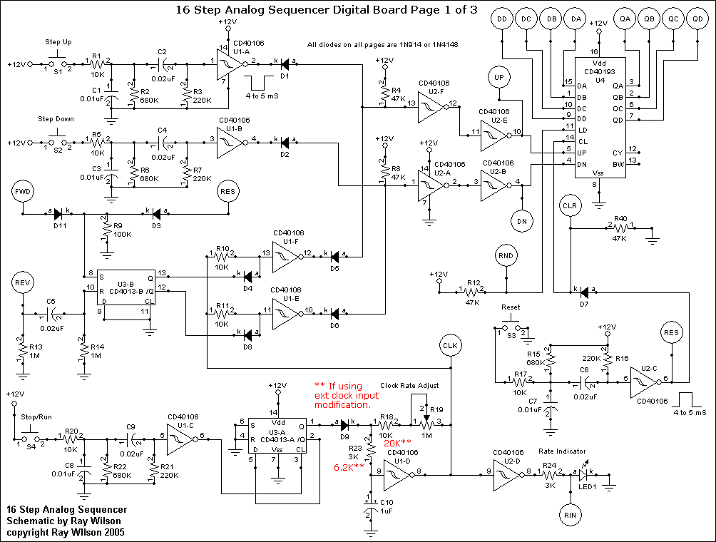
| Page 1 shows the clocking and counting section of the circuit. This part of the circuit controls the manual and automatic stepping of the sequencer. U4 counts up when
a positive going edge is applied to its UP input while its DN input is held high. Conversely it counts down when a positive going edge is applied to its DN input while the UP input is held high. If
the LD input is brought low the outputs of U4 (QA through QD) follow the data on the load inputs (DA through DD). When the sequencer is not in Random mode the LD input is held high via R12 to +12V.
A high level on the CL input of U4 causes the counter to reset to a count of zero.
S1 and associated components (R1, C2, C1, R2, R3, and U1-A) comprise a switch debouncer/low going pulser. When S1 is pressed a clean low going pulse of about 1 to 2 mS appears at the output of U1-A. In the same manner, S2 and its associated components and S4 and its associated components form switch debouncer/low going pulsers. S3 and its associated components work in the opposite fashion of S1, S2 and S4 in that when S3 is pressed a clean positive going pulse appears at U2-C pin 6. S3 is used soley to reset counter U4. The clock (square wave oscillator) for the sequencer is made up of U1-D, C10, R23, R18, and R19 (clock rate adjust). It runs when U3-A's Q output is low thus reverse biasing D9. Due to U1-D being a schmidt trigger inverter it can be made to oscillate by applying its output back to its input via a resistor and connecting a capacitor to its input. When the output is high it charges C10 via R19, R18, and R23 in series until its high threshold is reached at which time its output snaps low and C10 discharges through the same path until U1-D's low threshold is reached when its output snaps high and begins the cycle anew. The purpose of the value changes needed for the clock input modification is to raise the impedance of the external clock input node so that external clocking from sources with output impedance up to 1K can reliably clock the sequencer. A clean rectangular clock source oscillating between ground and +V is assumed. If an external clock source with negative voltage excursions is used then a diode must be placed between the input jack and pin 9 of U1-D. The anode of the diode goes to the jack's hot and the cathode goes to pin 9 of U1-D. If U3-A's Q output is high the clock is stopped (due to C10 being held fully charged via D9) and its output (U1-D pin 8) is forced low. Pressing S4 toggles the state of U3-A's Q output since U3-A is wired as a divide by two counter. Thus you can start or stop the clock by pressing S4. The clock signal is fed to the inputs of U1-F and U1-E via 10K resistors R10 and R11 respectively. D4 and D5 are used (in conjunction with U3-B) to control which of these inverters propogate the clock signal. U3-B is used to control the direction in which U4 counts. When the clock is running and U3-B's Q is high (and subsequently its NOT-Q is low) the clock pulses are allowed to propogate through U1-F but are stopped from passing through U1-E due to U1-E's pin 11 being pulled low via D8. When the clock is running and U3-B's Q is low (and subsequently its NOT-Q is high) the clock pulses are allowed to propogate through U1-E but are stopped from passing through U1-F due to U1-F's pin 13 being pulled low via D4. During operation U3-B's set and reset lines are pulsed appropriately to control the count direction. Notice that the anodes of D5 and D1 are connected to U2-F's input (pin 13). If either U1-A pin 2 or U1-F pin 12 go low then U2-F pin 13 is pulled low (via D1 or D5 respectively). When both U1-A pin 2 and U1-F pin 12 are high, U2-F pin 13 is held high via R4 (47K to +12V). Thus a push of S1 or a low to high transition of U1-F pin 12 can cause U4 to count up. Also note that U2-E pin 10 follows the state of U2-F's input (pin 13). Notice that the anodes of D2 and D6 are connected to U2-A's input (pin 1). If either U1-B pin 4 or U1-E pin 10 go low then U2-A pin 1 is pulled low (via D2 or D6 respectively). When both U1-B pin 4 or U1-E pin 10 are high, U2-A pin 1 is held high via R8 (47K to +12V). Thus a push of S2 or a low to high transition of U1-E pin 10 can cause U4 to count down. Also note that U2-B pin 4 follows the state of U2-A's input (pin 1). Normally the UP and DN inputs of U4 are held high. Low to high transitions are used on either UP or DN (while the opposite input is held high) to cause clocking in either direction. When the sequencer is running (i.e. U3-A's Q is high and neither "Step Up" or "Step Down" are being pressed) and U3-B's Q output is high (counting up) U4's DN clock input (pin 4) is held high (as explained above). Thus the counter counts up. This continues until the count is reached that corresponds with the setting of S9 (SP12T selector switch). Notice that U5 CD4514 (4-bit Latch/4-16 Line Decoder) is controlled by the counter (U4). The output that corresponds to the current counter's QA-QD outputs (one of S-0 through S-15) is high
while all of the others are low. U5's outputs S-4 through S-15 are connected to the poles of S9 (S-4 to 1, S-5 to 2, S-6 to 3 through S-15 to 12). This is to allow the sequence to reset or reverse
at the set step count. The common pole of S9 is controlled via switches S12, S15, and S16 to connect to:
Notice that any time the S-0 output of U5 goes high that U3-B is set (count up is set). This is so the counter starts to count up anytime the 0th count is reached. Thus if the sequencer is in "Reverse At Count" mode the sequencer will count up to the step setting of S9 and then reverse direction and count down toward 0. This is because the high going level seen at the REV connection is used to flip U3-B into the state that causes the counter to count down (U3-B's Q is low and U3-B's NOT-Q is high). When 0 is reached the count direction is set to up again. This cycle continues as the sequencer counts up and down until the mode is changed or the clock is stopped. If the sequencer is in "Reset At Count" mode the sequencer will count up to the step setting of S9 and then clear the counter to zero. The sequencer will continue to count from zero to count and reset until the mode is changed or the clock is stopped. "16 Step Sequence" mode is provided to allow the sequencer to repeat all 16 steps until the mode is changed or the clock is stopped. "Random 16" mode causes the counter to assume the count provided at the outputs of U8 CD4094 8 Channel Shift Register/Latch. The random counter is explained below. |
16 Step Analog Sequencer Digital Board Page 2 Click for PDF
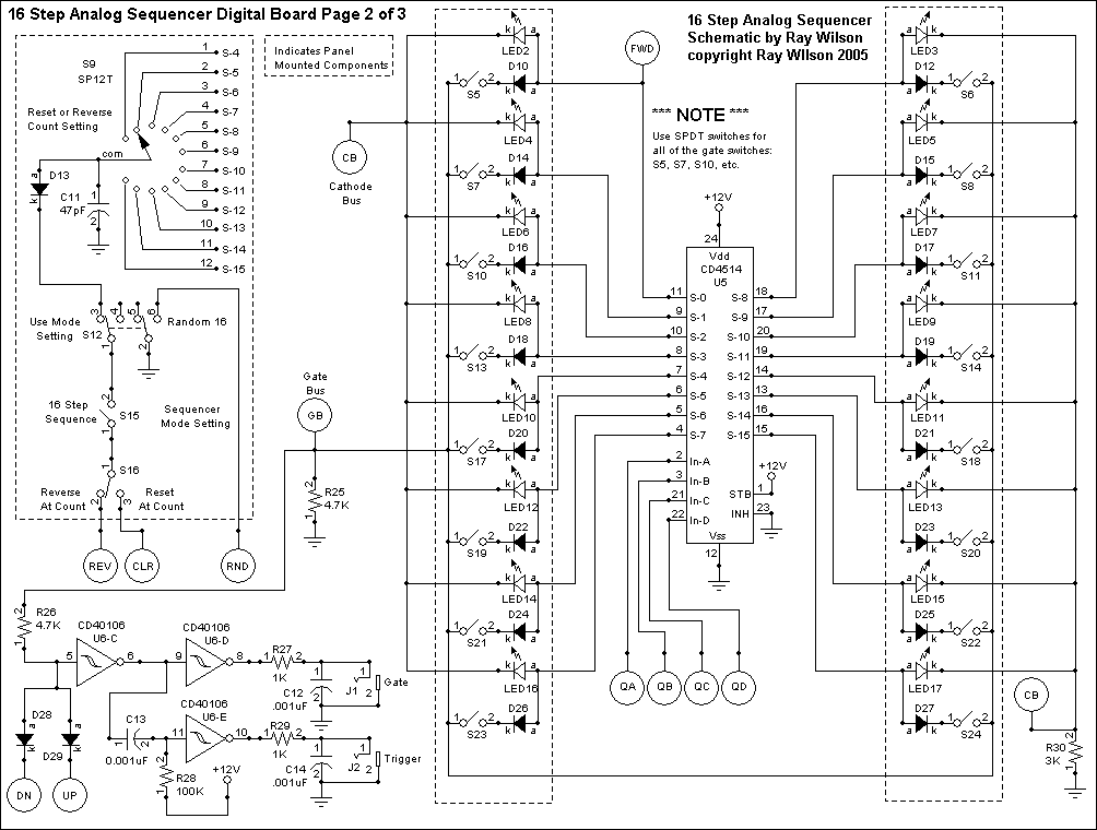
| As explained above U5's 16 outputs go high corresponding to the current count (0 thru 15) on the outputs of U4 (QA thru QD). They are used to power the LED
corresponding to the current step number. This LED lets you know which set of Coarse/Fine pots is the active one. Additionally each output (S0 thru S15) is fed to a switch and the anode of a diode
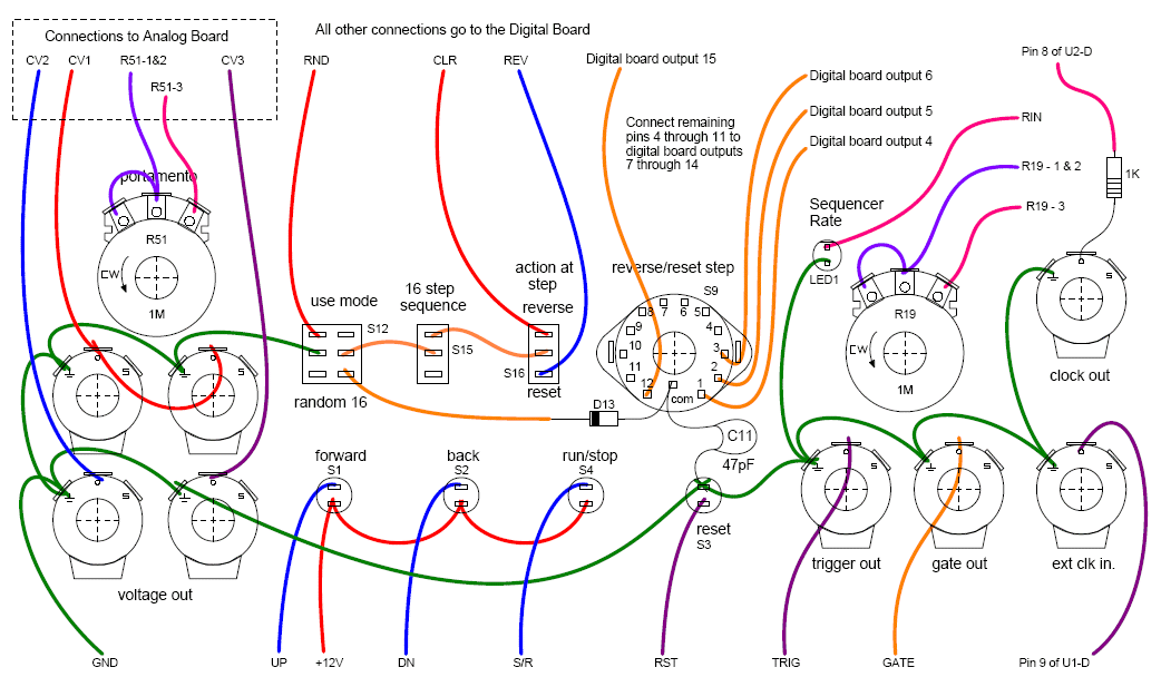
which is used to control at which steps gate/trigger outputs are produced. Essentially the outputs of U5 are anded with the clock signal if the switch for a particular step is closed. I recommend
using SPDT switches (even though the schematic shows SPST) to facilitate the panel wiring as shown in the panel wiring diagram. Note that both D13 and C11 are included in the panel wiring and are
not shown on the PC board. All of the LEDs, switches and the diodes connected to the outputs of U5 are also part of the panel wiring.
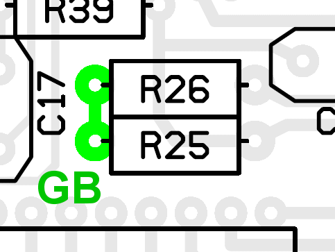
Gate Bus (GB) is not shown on the PC board. Details of where to connect GB are explained below in the PC parts layout section. |
16 Step Analog Sequencer Digital Board Page 3 Click for PDF
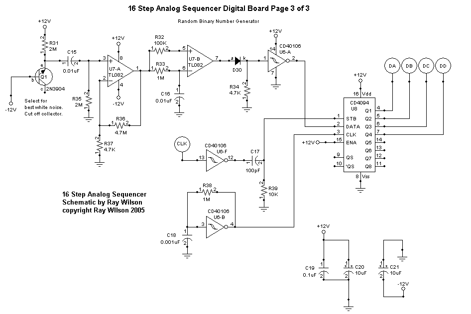
| This is the simplest way I could find to generate random binary numbers. These are truly random because they are based on white noise and not any repeating pattern. Feel free to use this circuit in your super computer. Essentially, white noise is generated by Q1 and amplified to digital levels by the op amps and U6-A. This noise data is presented to the input of the shift register who is constantly clocked by the oscillating output of U6-B. Thus random ones and zeroes are constantly flowing through the shift registers internal flip flop chain. A positive pulse that corresponds to the low going edge of the clock signal is applied to the strobe input of the CD4094 which causes whatever number is floating through the shift register to be latched and presented to its outputs (DA through DD). These outputs are connected to the data inputs of U4. When U4's pin 11 is held low (Random 16 mode selected) U4 propogates the random 4 bit count to U5 on each main clock cycle and thus the 16 steps are randomly selected. Tune the steps to the scale of your choice and select random mode to hear a never repeating random melody. |
**** Note on VS1 ****
VS1 - Reference Diode LM336-2.5 can be replaced with LM4040-2.5 since the LM336's adj. pin is not used.Search JAMECO for: IC,LM336BZ-2.5,TO-92, VOLT REFERENCE DIODE,2.5V
Search JAMECO for: IC,LM4040DIZ-2.5,TO-92, VOLT REF,PREC uPWR
Click to go to JAMECO
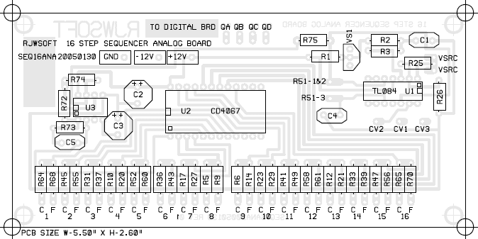
16 Step Analog Sequencer Analog Board Page 1 Click for PDF

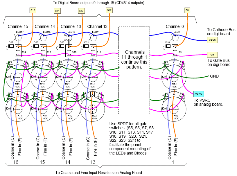
| This is the analog board schematic. The CD4067 16-channel Analog Multiplexer/Demultiplexer is used to direct the voltage set by the 16 sets of Coarse/Fine voltage adjustment to the CV outputs. The voltage generated by U1-A and associated components is dropped across all 32 of the pots which are used as voltage dividers feeding a summer amplifer. As the multiplexer's control inputs (QA through QD) change, the channel corresponding to the binary count is activated thus feeding the voltage from its associated Coarse/Fine pot pair to the summer. The coarse pot is fed to the summer via 100K and the fine pot is fed to the summer via 2M thus the range of adjustment is 1/20 that of the coarse control. I find that this give a good mix of range and fine tuning for the most demanding sequences. If you plan to use a value different from the recommended 100K remember that the load presented to the output of U1-A is Pot-Resistance/32. With 100K pots this is about 3125 ohms which a TL084 can drive quite well. Going up in value will be fine going down too far in value could overload the output of the TL084 causing unwanted inter-step voltage change effects. So I recommend you stay at or above 100K for the pots. |
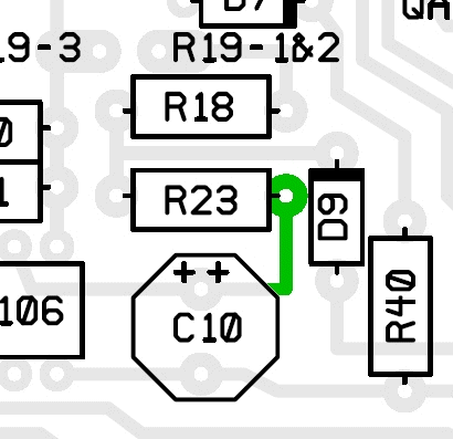
| I don't want to name names but someone forgot to put a connection point on the board for the Gate Bus (GB connection). This is not a big deal at all and is very easy to handle. There is no trace cutting or rewiring just a bit of creative component lead bending. Notice the highlighted section below. That is the circuit board point corresponding to the GB connection point. I suggest that you use the hole for R25 as the Gate Bus wire connection point and bend R25's lead to contact R26's lead and solder them together. As an alternative you could make R25's lead into a small loop or eyelet and put the Gate Bus wire through it and R25's lead hole and then solder the wire normally on the bottom of the board and then solder the eyelet and wire togther on the top of the board. Or... just install R25 and R26 normally and then loop the Gate Bus wire over R25's lead and solder it. Have I beat this subject to death yet? Everyone is probably saying "I get it" by now. Right, then... Just so you know we sent the responsible engineer on a hunt for "Medium Sized Foot" in the northwest mountains of the United States. |
 |
 |
 |
| Ext Clock Input | Clock Output | |
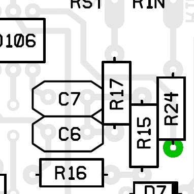
| Connect a wire to the junction of R23 and C10 positive terminal and connect it as shown below to obtain external clock input. The external clock will control the sequencer. The sequencer's Stop/Run control will have no effect. The expected impedance of the clock source is 1K or less. The clocking signal is assumed to be a clean ground to +V rectangle wave. If you want to use a clock source that goes from -V to +V you need to insert a diode between the input jack and the circuit point shown. The anode of the diode will go to the jack and the cathode of the diode will go to the circuit point shown. There is no legend or hole on the board for this wire and so you need to loop the wire, being careful not to short to surrounding components on the resistor lead shown. If using the "ext clock in" mod it is important to change the value of R23 to 6.2K and R18 to 20K. | Connect a wire to the junction of R24 and U2 pin 8 and connect it as shown below (via 1K resistor) to obtain clock output capability. The clock will start and stop via the Stop/Run control. The output clock signal is a clean ground to +V rectangle wave with capability to drive 10K ohm impedances effectively. There is no legend or hole on the board for this wire and so you need to loop the wire, being careful not to short to surrounding components on the resistor lead shown. | |
 |
 |
16 Step Analog Sequencer Digital Board Parts List
| Qty. | Description | Value | Designators |
|---|---|---|---|
| 3 | CD40106 Hex Schmidt Inverter | CD40106 | U1, U2, U6 |
| 1 | CD4013 Dual D Flip Flop | CD4013-A | U3 |
| 1 | CD40193 4 Bit U/D Counter | CD40193 | U4 |
| 1 | CD4094 8 Stage Shift/Store Reg | CD4094 | U8 |
| 1 | CD4514 4 Bit Latched 4 to 16 Dec. | CD4514 | U5 |
| 1 | TL082 Dual Op Amp | TL082 | U7 |
| 30 | 1N914 Diode(s) | General purpose high speed switching diode | D9, D2, D8, D4, D3, D5, D6, D7, D1, D11, D15, D12, D19, D17, D23, D21, D27, D25, D29, D28, D26, D24, D22, D20, D16, D18, D14, D10, D13, D30 |
| 1 | 2N3904 | 2N3904 | Q1 |
| 17 | General Purpose LED(s) | LED | LED1, LED5, LED3, LED9, LED7, LED13, LED11, LED17, LED15, LED4, LED2, LED8, LED6, LED12, LED10, LED16, LED14 |
| 4 | Ceramic Capacitor(s) | 0.001uF | C14, C12, C13, C18 |
| 6 | Ceramic Capacitor(s) | 0.01uF | C3, C1, C8, C7, C15, C16 |
| 5 | Ceramic Capacitor(s) | 0.02uF | C4, C9, C5, C6, C2 |
| 1 | Ceramic Capacitor | 0.1uF | C19 |
| 1 | Ceramic Capacitor | 100pF | C17 |
| 1 | Ceramic Capacitor | 47pF | C11 |
| 2 | Electrolytic Capacitor(s) | 10uF | C20, C21 |
| 1 | Tantalum Capacitor | 1uF | C10 |
| 1 | Linear Potentiometer | 1M | R19 |
| 3 | Resistor 1/4 Watt 5%(s) | 100K | R9, R28, R32 |
| 8 | Resistor 1/4 Watt 5%(s) | 10K (R18 20K if using clk mod) | R1, R20, R5, R11, R17, R18**, R10, R39 |
| 2 | Resistor 1/4 Watt 5%(s) | 1K | R29, R27 |
| 4 | Resistor 1/4 Watt 5%(s) | 1M | R14, R13, R33, R38 |
| 4 | Resistor 1/4 Watt 5%(s) | 220K | R3, R7, R21, R16 |
| 2 | Resistor 1/4 Watt 5%(s) | 2M | R31, R35 |
| 3 | Resistor 1/4 Watt 5%(s) | 3K (R23 6.2K if using clk mod) | R24, R23**, R30 |
| 4 | Resistor 1/4 Watt 5%(s) | 4.7K | R26, R25, R37, R34 |
| 1 | Resistor 1/4 Watt 5% | 4.7M | R36 |
| 4 | Resistor 1/4 Watt 5%(s) | 47K | R8, R4, R40, R12 |
| 4 | Resistor 1/4 Watt 5%(s) | 680K | R2, R6, R22, R15 |
| 4 | SPST PB Switch(s) | SPST | S1, S2, S4, S3 |
| 18 | SPDT Switch(s) | SPST | S5, S7, S10, S13, S17, S19, S21, S23, S6, S8, S11, S14, S18, S20, S22, S24, S15, S16 |
| 1 | DPDT Switch | DPDT | S12 |
| 2 | 1/4" Phone Jack(s) | Phone Jack | Gate and Trigger Jacks |
| 1 | Single Pole 12 Throw Rotary Switch (non-shorting) | SP12T | S9 |
16 Step Analog Sequencer Analog Board Parts List
| Qty. | Description | Value | Designators |
|---|---|---|---|
| 1 | CD4067 Analog Mux/DeMux | CD4067 | U2 |
| 1 | TL082 Dual Op Amp | TL082 | U3 |
| 1 | TL084 Quad Op Amp | TL084 | U1 |
| 1 | LM336 2.5V Ref. | LM336-2.5V | VS1 |
| 2 | Ceramic Capacitor(s) | 0.1uF | C1, C4 |
| 1 | Ceramic Capacitor | 470pF (used to be 10pF) | C5 |
| 2 | Electrolytic Capacitor(s) | 100uF | C3, C2 |
| 32 | Linear Potentiometer(s) | 100K | R11, R19, R32, R38, R46, R54, R63, R69, R4, R8, R18, R35, R44, R53, R62, R13, R22, R40, R34, R48, R57, R71, R66, R7, R15, R30, R24, R42, R50, R67, R59, R28 |
| 1 | Potentiometer | 1M | R51 |
| 18 | Resistor 1/4 Watt 1%(s) | 100K | R10, R31, R45, R17, R36, R12, R33, R47, R65, R6, R23, R41, R58, R5, R64, R26, R73, R52 |
| 3 | Resistor 1/4 Watt 1%(s) | 10K | R74, R72, R1 |
| 1 | Resistor 1/4 Watt 1% | 200K | R25 |
| 1 | Resistor 1/4 Watt 1% | 22 ohms | R75 |
| 16 | Resistor 1/4 Watt 1%(s) | 2M | R55, R27, R43, R20, R37, R68, R21, R39, R56, R70, R14, R29, R49, R61, R9, R60 |
| 2 | Resistor 1/4 Watt 1%(s) | 47K | R2, R3 |
Miscellaneous
- (3) 4" x 10" 1/16" thick Aluminum plate for mounting the pots and switches. Or one large aluminum (or 1/32" steel) panel 12" x 10" to mount everything.
- One Case to hold the unit (homemade wooden box, aluminum project box, etc)
- Assorted hardware 1" 6-32 nuts and bolts, 1/2" #8 wood screws, etc
- Knobs for potentiometers, wire, solder and typical assorted electronics hand tools.
- Digital Volt Meter and a Signal Tracer or oscilloscope for testing.