Ray Wilson authored this content while he was actively running MFOS as the founder and resident genius.
We retain the content because it reflects a valuable point of view representing that time and place.
Article by Ray Wilson
Introduction
This board is designed to work with the MFOS 16 Step Sequencer and supports both another set of "active step" LED indicators and another set of gate switches if that's something you want or need to build. So when you decide to expand your sequencer with another MFOS 16 Step Sequencer Analog board you'll want to add "active step" LED indicators and this board is perfect for that. Or maybe you want to build the Vari-Clock module into a separate cabinet because your sequencer cabinet is full... again you'll want to add "active step" LED indicators and this board is perfect for that. Or let's say you want another set of gate switches and another gate and trigger output and "active step" LED indicators... guess which board is perfect for that... BINGO! This is the very board. I will show the board as used in these two modes: 1) as another set of both LEDs and gate/trigger switches and 2) as just another set of LEDs.
Schematic Page 1 Description
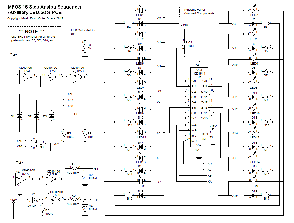
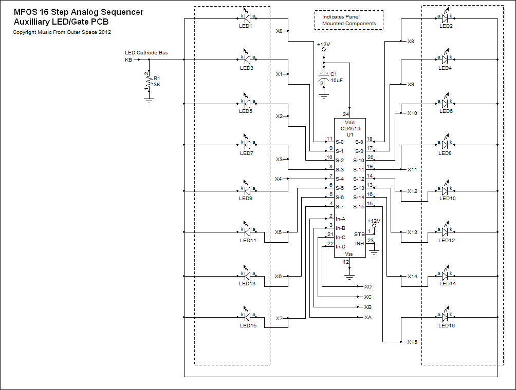
This is a very simple board and contains the circuitry for driving another set of "active step" LED indicators and/or another set of gate switches. U1 (CD4514 4-Bit Latched/4-to-16 Line Decoder) steers the high level needed to light the LEDs. One LED is powered at a time as the A thru D logic lines select a channel and a high logic level (+12V) is applied to it's anode. All LED kathodes are tied to ground through 3K resistor R1 at point KB (Kathode Buss). R1's value can be lowered if the LEDs need to be brighter but I would not go below about 1K. The QA thru QD connections from the MFOS 16 Step Sequencer Digital board must be connected to the corresponding XA thru XD connections of this board.
The gate logic is exactly the same as that used in the MFOS 16 Step Sequencer circuit with some very minor changes (no functional changes). As the MFOS 16 Step Sequencer steps through the various channels, the outputs of U1 (S-0 thru S-15) go high one after the other with no break. The switches in series with the diodes are used to control whether a gate is generated during a step. However when consecutive switches are on if you looked at the junction of all of the kathodes of D4 thru D19 with a scope you would notice that point GB remains high throughout all of the consecutive steps that have their gate switches on. Since we need the gate signal to go high on sequencer step change and then return low again before the next step change (so we can generate gate signals) we AND the outputs of the CD4514 with the clock signals from the MFOS 16 Step Sequencer or, if using the Vari Clock module, with the gate signals of that module (all interconnections are detailed below in diagrams and schematics).
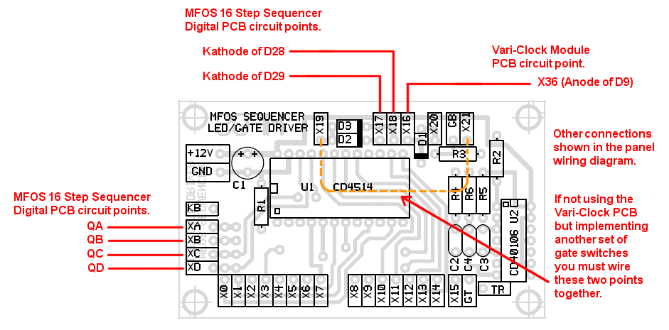
We feed the outputs of the CD4514 (basically logic signals going from ground to V+) via the diodes and switches to point GB where they are dropped on 10K resistor R3. The voltage dropped on R3 is fed through 100K resistor R2 to the input of U2-A CD40106 Schmitt Trigger inverter. The input of U2-A is very high impedance so the 100K resistor in series with it's input is hardly noticed by it. Diodes D1, D2 and D3 are used to pull the junction of U2-A pin 1 and 100K resistor R2 low whenever the signals connected to any of X16, X17 and/or X18 go to a logic low (ground potential). If any of the kathodes of D1, D2, or D3 are pulled to logic low (ground) they hold the input of U2-A at about .6V which is well below the Schmitt Trigger inverter's low threshold and thus U2-A's output goes to a logic high. In operation X17 (connected to kathode of D2) gets connected to the MFOS 16 Step Sequencer Digital Board's UP clock point. To access the MFOS 16 Step Sequencer Digital Board's UP clock point a wire needs to be soldered to the cathode of the MFOS 16 Step Sequencer Digital Board's diode D29. You can either carefully solder directly to the kathode lead of D29 or to D29's kathode's pad on the underside of the MFOS 16 Step Sequencer Digital PC board. In operation X18 (connected to kathode of D3) gets connected to the MFOS 16 Step Sequencer Digital Board's DN clock point. To access the MFOS 16 Step Sequencer Digital Board's DN clock point a wire needs to be soldered to the cathode of the MFOS 16 Step Sequencer Digital Board's diode D28. You can either carefully solder directly to the kathode lead of D28 or to D28's kathode's pad on the underside of the MFOS 16 Step Sequencer Digital PC board. If using the Vari-Clock circuit point X16 needs to be connected to the MFOS Vari-Clock module's point X36 which is the anode of the MFOS Vari-Clock PC board's D9. You can either carefully solder directly to the anode lead of D9 or to D9's anode's pad on the underside of the MFOS Vari-Clock PC board.
However when point GB is high and none of the kathodes of D1, D2 or D3 are being pulled low the input to U2-A is high and it's output is low. U2-B inverts the output of U2-A resulting in a high logic level at the output of U2-B. U2-B's output is connected in series with 100 ohm resistor R4 to the output Gate jack which is in parallel with glitch suppressor C2 .001uF ceramic cap. As U2-A's output goes low due to the high level on it's input, current is pulled momentarily through C3 .001 uF ceramic cap briefly bringing U2-C's input momentarily low. R5 quickly recharges the side of C3 facing U2-C's input and the output of U2-C goes low after being high for a few milliseconds. U2-C's output is connected in series with 100 ohm resistor R6 to the output Trigger jack which is in parallel with glitch suppressor C4 .001uF ceramic cap.
If you are just using the board to support another set of "active channel" LEDs then there is no need to put the following parts on the board at all:
- U2 - CD40106
- All diodes D1 thru D19
- Resistors R2, R3, R4, R5, R6
- Capacitors C2, C3, C4
- Switches S1 thru S17 are not used.
Schematic: PCB Used for LEDs and Gate Switches
View as PDFWhen the board is populated to support both another set of "active step" LEDs and another set of gate switches this is the corresponding schematic diagram.
Schematic: PCB Used for LEDs only
View as PDFWhen the board is populated to support "active step" LEDs only this is the corresponding schematic diagram.
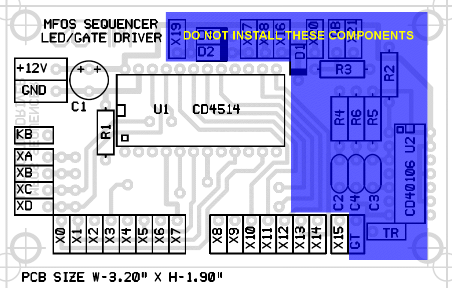
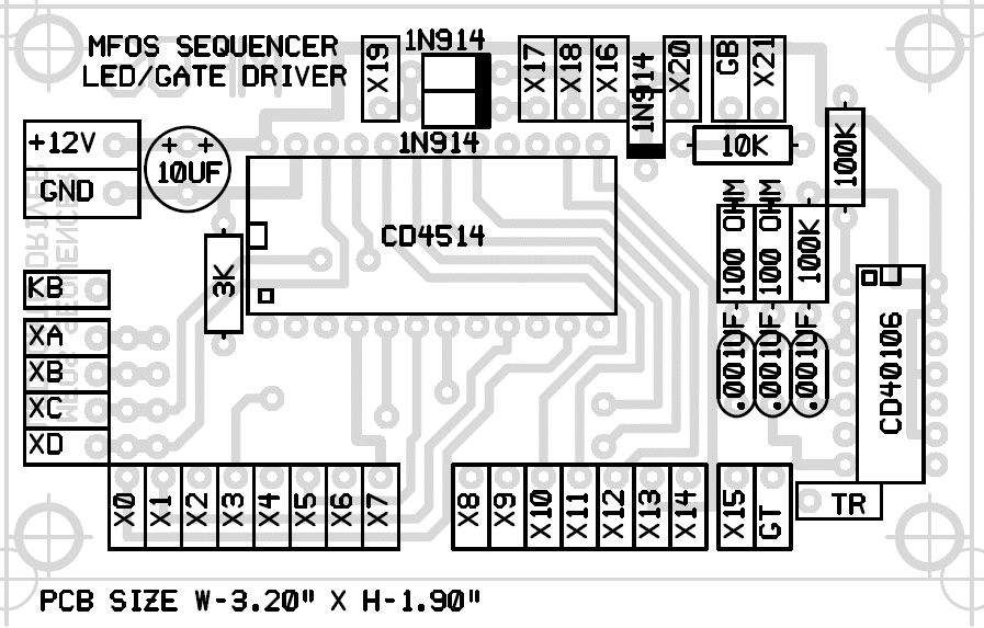
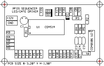
16 Step Sequencer Auxiliary LED Driver ONLY PCB Designators
Use this view during board troubleshooting where you will need to associate legend names with schematic values and component interconnections. There is a value view below so don't break your neck going between the schematic and the PCB during assembly. Do not install the components in the shaded area if using the board solely for driving another set of LEDs.
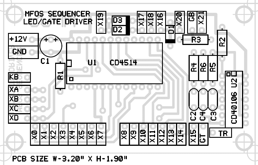
16 Step Sequencer Auxiliary Gate Switch and LED Driver PCB Designators
Use this view during board troubleshooting where you will need to associate legend names with schematic values and component interconnections. There is a value view below so don't break your neck going between the schematic and the PCB during assembly.
16 Step Sequencer Auxiliary GATE/LED Driver PCB Values
Use this view during board population so you don't have to keep referring to the schematic to see what value relates to each designator. Remember that you don't install several of these components if using the board to support active step LEDs only. Just stuff the board with the values for the intended use of the PCB and voila... you're good to go.
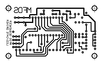
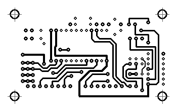
16 Step Sequencer Auxiliary GATE/LED Driver PCB Layouts
Bottom Copper
If you use these layouts experiment with your drawing program's scaling until when printed the IC pad centers 0.1" apart and 0.3" across for the 14 pin DIP packages and 0.6" across for the 24 pin DIP packages (all scaling will be correct once that is achieved).
Top Copper
Legend Silk Screen
16 Step Sequencer Auxiliary GATE/LED Driver PCB Parts Lists
All integrated circuits need to be DIP packages. When shopping for chips remember that the numbers will have suffixes like BE or BC but as long as they are DIP packages you will be fine. The suffixes typically indicate temperature ranges and package materials (plastic, ceramic, etc).
16 Step Sequencer Auxiliary LED Drivers ONLY PCB Parts List
If using the board for driving LEDs only then you only need to purchase these parts.
| Qty. | Description | Value | Designators |
|---|---|---|---|
| 1 | CD4514 4 Bit Latched 4 Dec. | CD4514 | U1 |
| 16 | General Purpose LED | LED | LED1, LED2, LED4, LED6, LED8, LED10, LED12, LED14, LED16, LED3, LED5, LED7, LED9, LED11, LED13, LED15 |
| 1 | Resistor 1/4 Watt 5% | 3K | R1 |
| 1 | Capacitor Electrolytic | 10uF | C1 |
16 Step Sequencer Auxiliary GATE and LED Driver PCB Parts List
If using the board for driving LEDs and a second set of gate switches you will need these parts.
| Qty. | Description | Value | Designators |
|---|---|---|---|
| 1 | CD40106 | CD40106 | U2 |
| 1 | CD4514 4 Bit Latched 4 Dec. | CD4514 | U1 |
| 19 | 1N914 Switching Diode | 1N914 | D1, D2, D3, D4, D5, D6, D7, D8, D9, D10, D11, D12, D13, D14, D15, D16, D17, D18, D19 |
| 16 | General Purpose LED | LED | LED1, LED2, LED4, LED6, LED8, LED10, LED12, LED14, LED16, LED3, LED5, LED7, LED9, LED11, LED13, LED15 |
| 2 | Resistor 1/4 Watt 5% | 100 ohm | R4, R6 |
| 2 | Resistor 1/4 Watt 5% | 100K | R2, R5 |
| 1 | Resistor 1/4 Watt 5% | 10K | R3 |
| 1 | Resistor 1/4 Watt 5% | 3K | R1 |
| 1 | Capacitor Electrolytic | 10uF | C1 |
| 3 | Ceramic Capacitor (S) | .001uF | C2, C3, C4 |
| 17 | SPDT Switch | SPDT | S1, S2, S3, S4, S5, S6, S7, S8, S9, S10, S11, S12, S13, S14, S15, S16, S17 |
16 Step Sequencer Auxiliary GATE/LED Driver Panel Wiring
View as PDFAs you can see this wiring diagram covers both modes of operation (LED driver only or LED driver and additional set of gate switches). This is totally illustrative and as long as you get the wiring correct the form factor does not matter. The horizontal line on the page divides the two implementations. Click image for a much larger one or view as a scalable PDF.
If you are adding another set of gate switches but you are not using the Vari-Clock circuit there is no need to add switch S1 or it's connections to the front panel. There is also no need to connect this PC board's point X16 to anything. However a wire must be placed on this PC board to connect points X21 and X19 (which connects the anodes of D2 and D3 directly to the input of U2-A). The points X17 and X18 must still be connected as shown in the diagram below for the gates provided by this board to function properly.
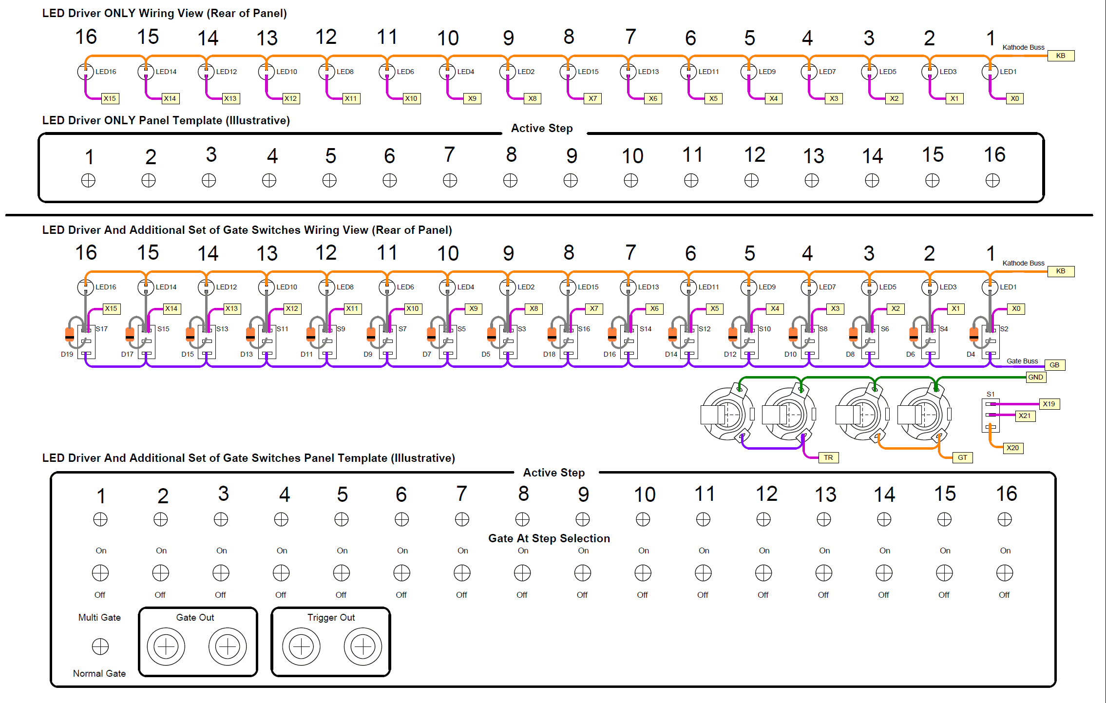
Here you see the connections necessary to have the LEDs and/or Gates function properly. Connecting this board's XA thru XD to the MFOS 16 Step Sequencer Digital Board's QA thru QD is required regardless of whether you plan to use the board for LEDs only or Gate Switches and LEDs. The other connections shown are necessary if you desire another set of gate switches. As mentioned above if adding another set of gate switches but not using the Vari-Clock PC board you do not need to connect this board's X16 to anything and you will not need switch S1 (shown in the wiring diagram) but a wire must be placed on this PC board to connect points X21 and X19.
If only adding another set of "active step" LEDs only the QA thru QD connections must be made as well as the connections shown in the wiring diagram for the LED only implementation. NOTE: The wire jumper is only needed if adding gate switches without the use of the Vari-Clock PCB.