Ray Wilson authored this content while he was actively running MFOS as the founder and resident genius.
We retain the content because it reflects a valuable point of view representing that time and place.
Article by Ray Wilson
The value of R7 has been changed from 1M to 10M. Doing so reduces the current through R7 and subsequently increases the precision of the bus voltage when a key is pressed. A voltage divider exists between the resistor ladder and R7. By increasing the value of R7 by a factor of 10 the output of the resistor ladder is loaded less (by 10X) when a key is pressed.
Features
- One Volt Per Octave Keyboard Controller
- Requires Only Single Buss Keyboard (or other single switch per note mechanism)
- Four CV outputs
- Two Outputs With Glide
- Trigger and Gate Outputs
- LED Drive For Gate And Trigger Indicators
- Great For Performance Art projects
- A True Classic Analog Synth Design
Can't Find a Single Buss Keyboard - Make Your Own!
Check out this totally cool idea...
Introduction
This old-school, vintage style single buss 1V/octave keyboard controller is very versatile. As a normal keyboard all you need is an old organ keyboard that has one switch per key that closes to a common buss. Or you can modify an old piano keyboard section with reed switches and magnets to make you own keyboard. Or mount reed switches on yourself or whatever and make a really cool looking controller that you play with magnets glued to your fingers for your next performance art gig. As long as you have a series of resistors with switches to close the junctions to a common bus you have a controller that can use this circuit to sample and hold key presses.

Sample & Hold Performance - Output Voltage Droop
The control voltage output of any analog based keyboard that uses a sample and hold which stores a voltage on a capacitor will eventually droop as any leakage path to the capacitor will eventually cause it to do so. These numbers represent what I believe is typical performance for this keyboard controller circuit when used with a .01uF polystyrene cap for C19 and the LF444CN for IC U3. It is important to clean ionic soils from the PC board using flux remover especially in the vicinity of these components as well as the 2N5457 sample switch transistors Q2 and Q3.
Third C up pressed: Ideal Voltage 2.000V
| Keydown | 2.0038V |
| 30 seconds later | 1.9972V |
| 30 seconds later | 1.9897V |
| 30 seconds later | 1.9819V |
| 30 seconds later | 1.9748V |
| 30 seconds later | 1.9672V |
| 30 seconds later | 1.9598V |
MIDI to CV modules do not suffer from output voltage droop and neither does the diode matrix keyboard project found on the site. I don't sell a PC board for the diode matrix circuit and it requires a dedicated switch per key (not switched to a buss) to function.
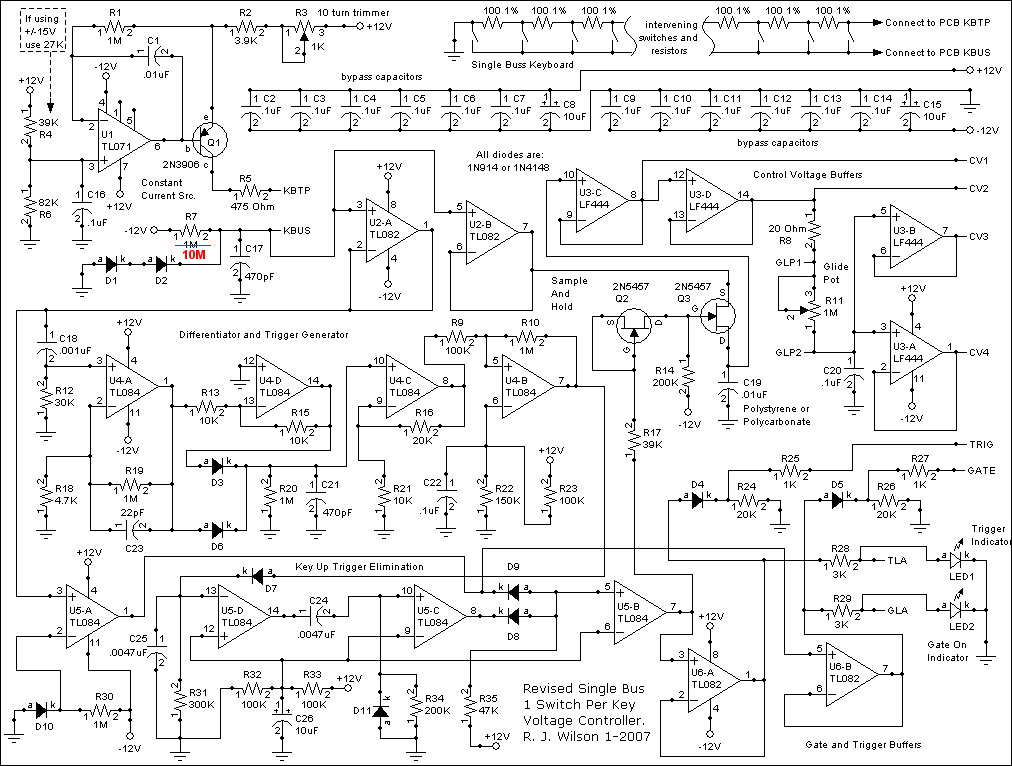
Single Buss 1V/Octave Keyboard Schematic Page 1 PDF
|
U1, Q1 and associated components comprise a constant current source. This circuit is based on the National Semiconductor data book entry for a constant current generator based around the LM3900. Lo and behold it works just fine with the TL071. If you are using +/-15V power supply change R4 to 27K. The current through Q1 stays the same regardless of load (within reason) with a 37 note keyboard it is loaded with 3.6K (36 100 ohm resistors) plus the 475 ohm resistor R5 for a total of 4.075K. When you press one note at a time the load on the constant current source does not change but when you press more than one key at a time the load presented to it changes due to the fact that you are shorting the resistors between the two pressed keys. This is a monophonic keyboard i.e. you only get one output of 1V/octave from the keyboard. When two keys are pressed the lower note takes precedence. This is due to the current being constant. The voltage output by the keyboard is .833 mA times the value of resistance you drop it across to ground. The lowest note of the keyboard will put out 0 volts because it shorts the buss to ground. The next note will put out 100 ohms times .833 mA or 83.3mV. The next note 200 ohms times .833 mA or 166.6 mV. The 13th note will put out 1200 * .833 mA or 999.6 mV (thus one volt per octave). As keys are pressed the voltage dropped across the resistor chain is presented to the common buss. The buss assumes the voltage presented to it by the switch. With no keys pressed the buss sits at about -.83 volts. Two diodes drops through 10M resistor R7 to -V below ground. The 10M resistor does not turn the diodes on very hard and thus you don't see the full two diode drops you might expect (i.e. -1.2V). The purpose of holding the buss below ground is to cause a change in voltage whenever any key is pressed (including the lowest key which grounds the buss) in order to develop a trigger/sample pulse from it. Whether you are playing one note at a time or holding a note and playing other notes a trigger/sample pulse is generated when a new note is pressed. The buss voltage is buffered by U2A and U2B. U2B's output feeds the differentiator responsible for developing a pulse whenever the buss voltage changes (a note is pressed or the keyboard is played legato). We differentiate the voltage by connecting to U4A through capacitor C18 (.001 uF) and dropping the voltage through it onto 30K. Only the leading and trailing edges of any rapidly changing voltage are passed through C18. U4A has a gain of about 2100 which amplifies the edges passing through C18. When a key is pressed and released the pulses at the output of U4A are the op-amp saturation level (approx. +/-10.5V). When adjacent notes are pressed in legato fashion the pulses are in the +/- 6V range. This is because there is always a buss voltage change of at least .83 volts when notes are pressed and released but only a change of .083 volts when adjacent keys are played legato. The positive excursions of U4A are dropped across R20 (1M resistor) via D6. The output of U4A is inverted by U4D. U4D's positive excursions (U4A's negative excursions) are dropped across R20 via D3. Thus the output of U4A is rectified and whether the voltage change is positive or negative at the input of U4A a positive spike is dropped across R20. The spikes are also presented to capacitor C21 which discharges via R20. The purpose of the C21 and R20 is to reduce the incidence of false triggering/sampling caused by noisey key contacts. While developing this circuit I used the crudest keyboard contacts I could (strips of circuit board closing to a common piece of circuit board) to insure that the design tolerated it. Even with this crude setup the incidence of false triggering/sampling was extremely rare. U4 and associated resistors provides a bit of gain (x3) to insure that the pulses from U4D are always close to or at the op-amps saturated voltage (about 10.5 volts). U4B is an op amp wired as a schmidt trigger (comparator with hysteresis) which is essentially the final pulse that indicates that a note has changed. A problem that needs to be solved with this kind of keyboard is how to prevent a trigger/sample from occurring when all notes are released. This is because the final release causes the buss to change voltage to the no-key pressed voltage (-.83 volts). If this was sampled the keyboard would emit a low note and trigger every time you released all the keys. To prevent this we delay the sampling pulse so that it occurs approximately 1 mS after a key is pressed or released. By ANDing the sample pulse with the gate which begins as soons as a key is pressed and ends as soon as all keys are released we achive our goal. The gate signal is generated by U5A wired as a comparator. Notice that U5A's inverting input is held at about -.419 volts by the single diode (D10) to -12V through 1M resistor R30. Now when no keys are pressed the buss voltage is -.83V well below the threshold of U5. When any key is pressed the voltage goes to at least ground (well above the threshold for U5A). Thus when any key is pressed the output of U5A goes high and when all keys are released the output of U5A goes low immediately. Now let's follow the change in voltage detector pulse from U4B pin 7. This pulse is presented to the non-inverting input of U5D (wired as a comparator) via D7. U5D's non-inverting input is held at 1/2 the positive supply (created by R32, R33 and C26). U5D's inverting input is normally held at ground by R31. Thus normally U5D's output is at the op amp's positive saturation voltage (about 10.5V). When a voltage change detector pulse occurs it charges C25 (.0047uF cap) via D7. When U4B returns low C25 discharges via R31. For the time that the voltage on C25 is above the threshold voltage on U5D's non-inverting input, U5D's output is at the negative saturation voltage of the op-amp (around -10.5V). U5D's output stays low (around -10.5V) for about 1mS every time the voltage change detection pulse fires. After that it shoots back to about +10.5V. The rising edge of U5D's output returning high is coupled through C24 onto R34 and D11. D11 suppresses the effect of the falling edge so that the comparator U5C does not trigger on it. The time constant of the coupled rising edge is such that the output of U5C goes high (10.5V) for about 1 mS on the rising edge of the U5D's low pulse. The 1mS low to high pulse on U5C's output is ANDed with the gate pulse from U5A via diodes D9 and D8. When both cathodes are high (Gate present and trigger present) U5B's output goes high. The outcome is that U5B only outputs a trigger/sample pulse whenever the gate is high (a key is down). When all keys are released the gate shoots low immediately but the final positive pulse from U5C occurs 1mS after the gate goes low so it is inhibited from causing U5B's output to go high. Thus when you release all keys no trigger or sample pulse occurs. The trigger/sample pulse is fed to buffer U6A whose output feeds both the trigger out (TRIG) and the trigger LED anode out (TLA). The Gate signal is fed to the gate buffer U6B whose output feeds both the Gate out (GATE) and the Gate LED anode out (GLA). Both the gate and the trigger go through diodes so that only the positive excursion of the respective signal is passed to the output. Gate and trigger pulses go from ground to the saturation voltage of the respective buffers (about 10.5 volts). The trigger/sample pulse is fed to the gate and source of NFET Q2. Q2's drain is connected to the gate of NFET Q3. The gate of Q3 is pulled low via R14 200K to -12V. Thus the voltage on the source of Q3 only charges the sample cap (.01 uF polystyrene cap C19) when the sample pulse is high. Q2 acts like a super low leakage diode which only conducts when the sample pulse is high. The buss voltage is presented to the source of Q3 and charges C19 during the sample pulse. When Q3 shuts off the voltage on the cap has no path for current to discharge it and so it stays charged (thus the term sample and hold). OK... I'll quit saying thus. The voltage on C19 is presented to the input of the high impedance non-inverting input of U3C. Since U3C's input is such a high impedance and JFET type op amps have such low input leakage the cap stays at the sampled voltage until another sample is taken (a key is pressed or the current note is changed). The output of U3C feeds follower U3D. The outputs U3C and U3D respectively feed CV1 and CV2 outputs. The output of U3D feeds the non-inverting inputs of U3B and U3A via R8 and the glide adjust pot R11. The glide adjust pot changes the time voltage changes take to charge or discharge C20 and so a glide or portamento effect is produced on the voltage output at CV3 and CV4. Calibration is easy. This procedure assumes that you have the circuit connected to the keyboard resistor chain, one end going to circuit board point KBTP (keyboard top) and the other end going to ground. We want to have .8333 mA flowing through the keyboard resistor chain which means that .8333 mA will be flowing through R5 (475 ohm 1% metal film resistor). When .8333 mA flows through a 475 ohm resistor is causes a (.0008333 Amp x 475 ohms) 0.3958175 volt drop across R5. So with the highest impedance most accurate DVM you have adjust R3 until you have 0.3958 volts across R5 and voila you will have .8333 mA flowing through the resistor chain which in turn will give you 1 volt per octave from your keyboard controller. |
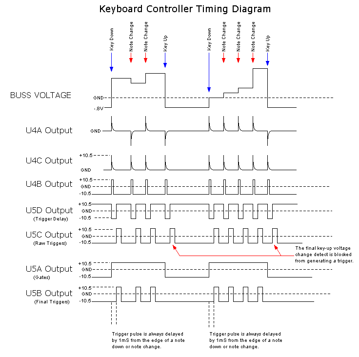
Single Buss 1V/Octave Keyboard Timing Diagram PDF
| Approx. Current Consumption | |
| +12V | 30mA |
| -12V | 30mA |
My Trusty Noisy Keyboard Switch Simulator Larger Image

Can't Find a Keyboard - Make Your Own!
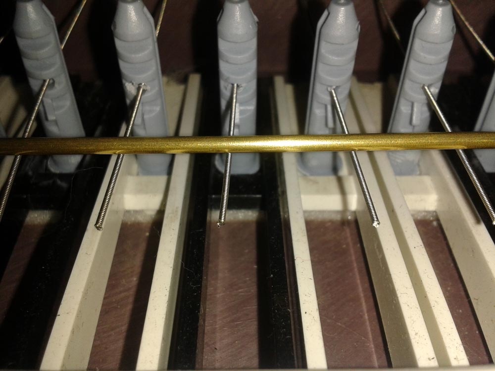
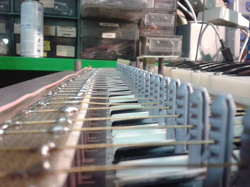
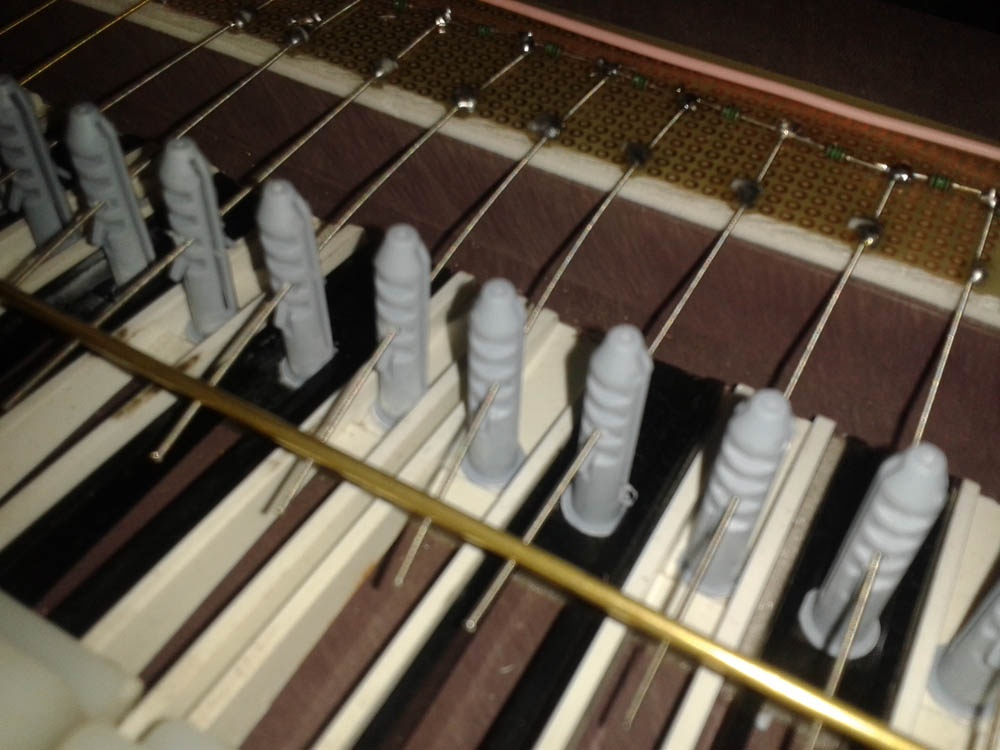
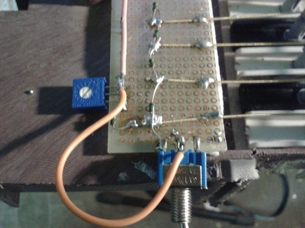
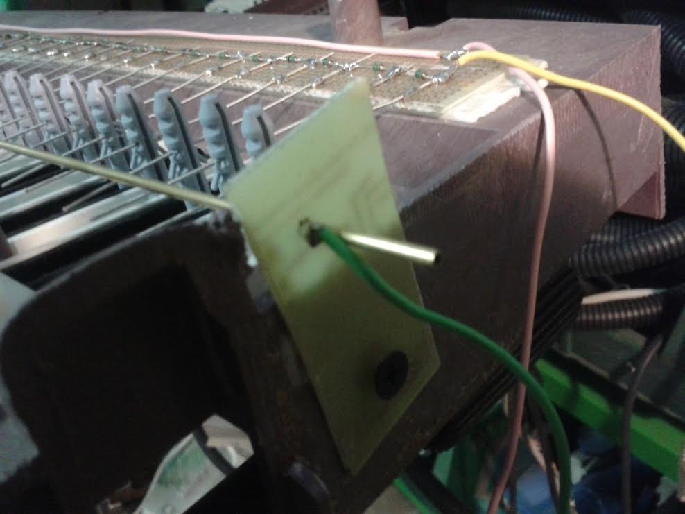
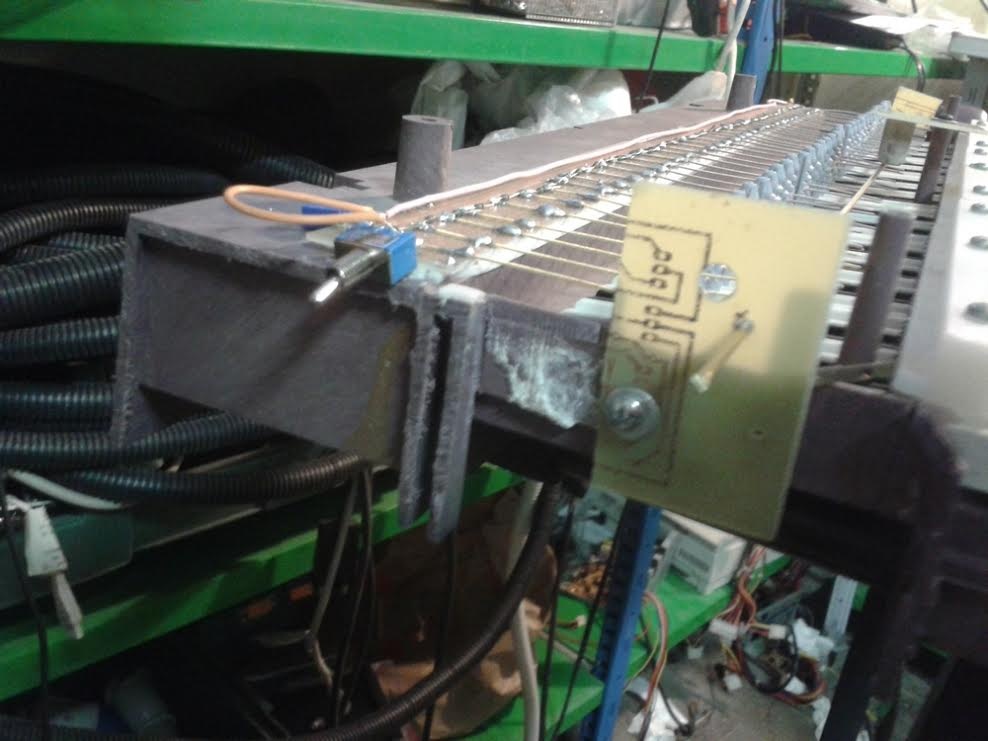
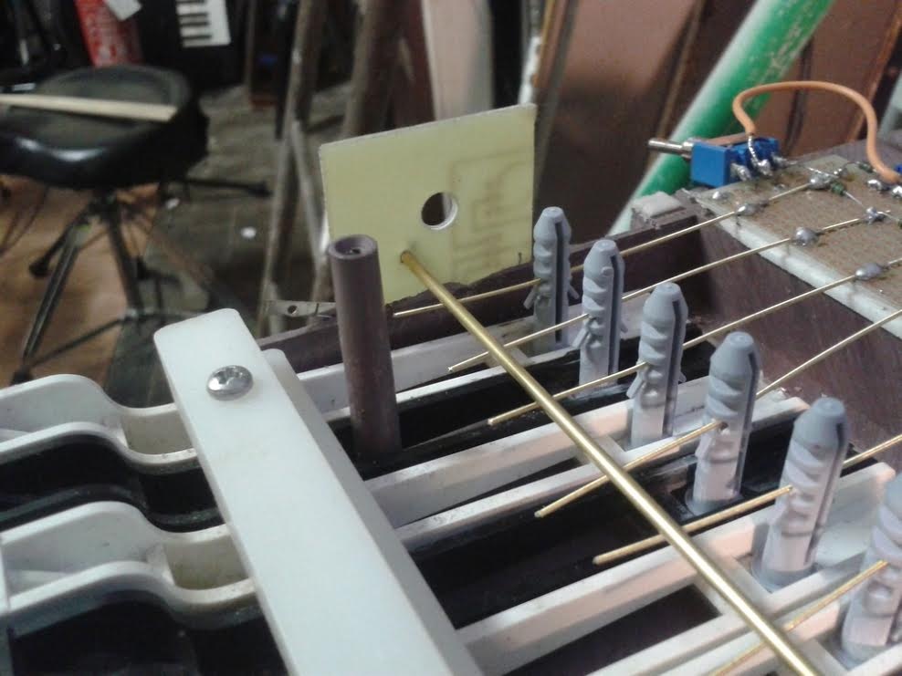
Getting keyboards is never a problem but adding the type of switch arrangement needed for a single bus keyboard controller can be. Diyer Francesco Bonaccorso shows a solution to the problem of the scarcity of keyboards that have spring contacts closing to a common bus. He used a toy organ built in the 70's that worked like an accordion to obtain only the keys.He used guitar strings as contacts and plastic expansion anchors, in which he drilled a hole, to pass the string through and a brass bar for the bus. I imagine that the plastic anchors are glued to the key bottoms with an adhesive (hot glue, contact cement, etc). The brass rod must be hung in a manner that insulates it from other circuit elements and still allows the key contacts to touch it when they are depressed to about 3/4 of their vertical travel.
These pictures tell the story quite nicely. I noticed that wound guitar strings were used for the key spring contacts. Perhaps using the lighter gauge non-wound strings would improve the contacting surfaces.
Thanks Francesco for this brilliant solution.
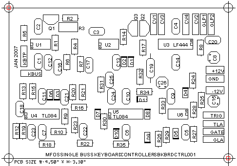
Single Buss 1V/Octave Keyboard PCB Parts Layout (Parts Side Shown) PDF
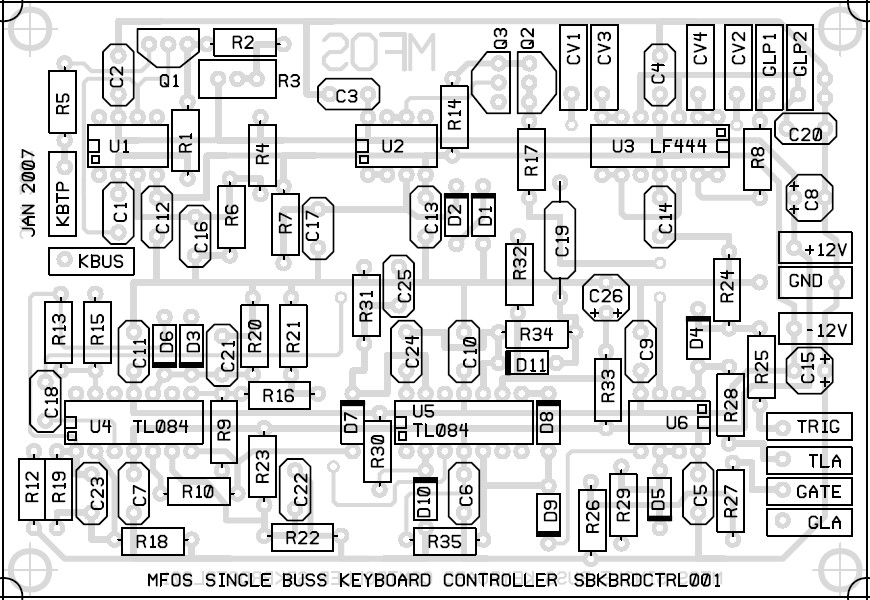
Single Buss 1V/Octave Keyboard PCB Part Values Layout (Parts Side Shown)

Single Buss 1V/Octave Keyboard PCB Bottom Copper (Parts Side Shown)
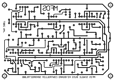
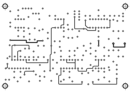
Single Buss 1V/Octave Keyboard PCB Top Copper(Parts Side Shown)
Single Buss 1V/Octave Keyboard PCB Top Silk Screen
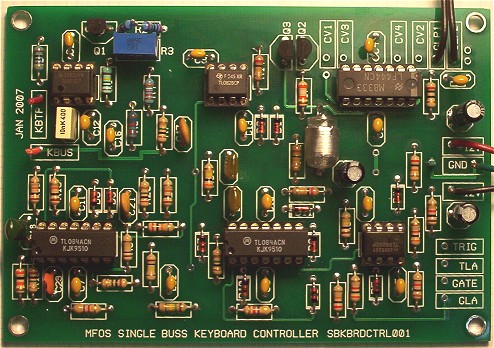
Single Buss 1V/Octave Keyboard PCB Populated Larger Image
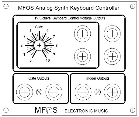
Single Buss 1V/Octave Keyboard Front Panel PDF
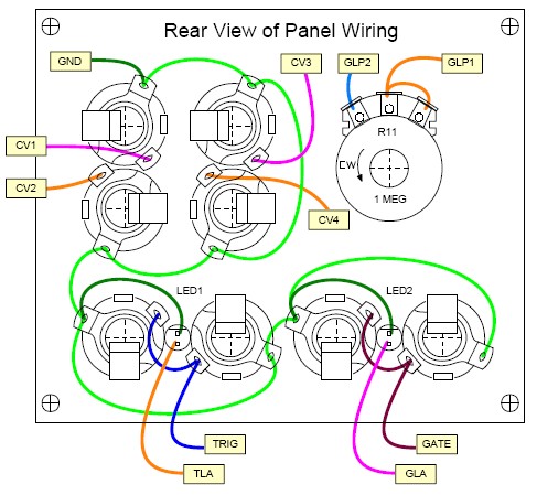
Single Buss 1V/Octave Keyboard Panel Wiring Rear View PDF
Single Buss 1V/Octave Keyboard Project Parts List
- Using 1% metal film resistors everywhere will reduce temperature related drift.
- Where 1% metal film is specified 5% carbon comp will work but with more temperature drift.
- Usually biFET amps (quads, duals, singles) can be replaced with an equivalent from another manufacturer.
- Capacitors can be film, ceramic, or silver mica.
- LM13700 subs (if applicable) (LM13600, NE5517, AU5517, NTE870).
Single Buss 1V/Octave Keyboard Project Parts List
| Qty. | Description | Value | Designators |
|---|---|---|---|
| 1 | LF444 Quad Op Amp | LF444 | U3 |
| 1 | TL071 Op Amp | TL071 | U1 |
| 2 | TL082 Dual Op Amp(s) | TL082 | U6, U2 |
| 2 | TL084 Quad Op Amp(s) | TL084 | U4, U5 |
| 11 | 1N914 or 1N4148 Sw. Diode(s) | Diode | D3, D10, D6, D8, D9, D5, D4, D7, D11, D2, D1 |
| 1 | 2N3906 PNP | 2N3906 | Q1 |
| 2 | 2N5457 NFET(s) | 2N5457 | Q3, Q2 |
| 2 | LED(s) | LED | LED2, LED1 |
| 1 | Linear Potentiometer | 1M | R11 |
| 4 | Resistor 1/4 Watt 1%(s) | 100K | R9, R23, R32, R33 |
| 3 | Resistor 1/4 Watt 1%(s) | 10K | R13, R15, R21 |
| 1 | Resistor 1/4 Watt 1% | 150K | R22 |
| 2 | Resistor 1/4 Watt 1%(s) | 1K | R27, R25 |
| 5 | Resistor 1/4 Watt 1%(s) | 1M | R20, R10, R30, R19, R1 |
| 1 | Resistor 1/4 Watt 1%(s) | 10M | R7 |
| 3 | Resistor 1/4 Watt 1%(s) | 20K | R16, R24, R26 |
| 1 | Resistor 1/4 Watt 1% | 20 Ohm | R8 |
| 1 | Resistor 1/4 Watt 1% | 3.9K | R2 |
| 1 | Resistor 1/4 Watt 1% | 300K | R31 |
| 1 | Resistor 1/4 Watt 1% | 30K | R12 |
| 1 | Resistor 1/4 Watt 1% | 39K | R4 |
| 2 | Resistor 1/4 Watt 1%(s) | 3K | R28, R29 |
| 1 | Resistor 1/4 Watt 1% | 4.7K | R18 |
| 1 | Resistor 1/4 Watt 1% | 475 Ohm | R5 |
| 1 | Resistor 1/4 Watt 1% | 47K | R35 |
| 1 | Resistor 1/4 Watt 1% | 82K | R6 |
| 2 | Resistor 1/4 Watt 5% | 200K | R14, R34 |
| 1 | Resistor 1/4 Watt 5% | 39K | R17 |
| 1 | Trim Pot | 1K | R3 |
| 1 | Capacitor Ceramic | .001uF | C18 |
| 2 | Capacitor Ceramic(s) | .0047uF | C25, C24 |
| 1 | Capacitor Ceramic | .01uF | C1 |
| 15 | Capacitor Ceramic(s) | .1uF | C22, C5, C6, C7, C9, C11, C10, C12, C13, C14, C2, C16, C20, C3, C4 |
| 1 | Capacitor Ceramic | 22pF | C23 |
| 2 | Capacitor Ceramic(s) | 470pF | C21, C17 |
| 1 | Polycarbonate or Polystyrene (low leakage) Capacitor | .01uF | C19 |
| 3 | Electrolytic Capacitor(s) | 10uF | C26, C8, C15 |
Miscellaneous
- 1/16" Thick aluminum plate for mounting the pots and switches.
- Unit is typically mounted in a synth case with other synth modules.
- Assorted hardware 1" 6-32 nuts and bolts, 1/2" #8 wood screws, etc
- Knobs for potentiometers, wire and solder.
- Digital Volt Meter and a Signal Tracer or oscilloscope for testing.