Ray Wilson authored this content while he was actively running MFOS as the founder and resident genius.
We retain the content because it reflects a valuable point of view representing that time and place.
Article by Ray Wilson
Features
- Sample Rates from .05HZ to 1KHZ.
- Voltage Controlled Sample Clock
- Clock Sync-In Can Double As External Clock In
- Glide Control To Slew Between Samples.
Introduction
Sample and hold circuits are used to create repeating or non-repeating cycles of control voltage by sampling a signal fed into the input at a rate set by the sample clock. At each sample the input voltage is stored on a capacitor and held there until the next sample. The held voltage is fed to the output which is used to control another module. It is interesting to sample various waveforms and hear the remarkable patterns that emerge as you vary the sample frequency or the frequency of the sampled signal. When noise is sampled then random non-repeating patterns are output.
Sample And Hold With VC-Clock MP3 Samples
Paolo of Italy's S&H saying Ay yay yay yay... Paolo's S&H saying Doh-wit Doh-wit. Paolo's S&H modulating a Ramp oscillator. Paolo's S&H modulating a Sine oscillator. Paolo's S&H modulating a Triangle oscillator. Paolo's S&H modulating a Sine oscillator (w/Portamento). Paolo's S&H modulating a Square Wave oscillator. Paolo's S&H demo of rate range.
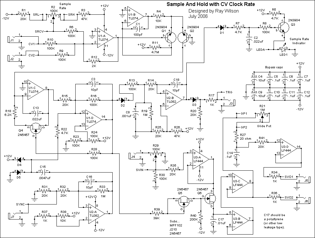
Sample And Hold With VC-Clock Schematic Page 1 PDF
|
Op amps U1-A, U1-B and associated components comprise a linear voltage to exponential current converter. It is used to control the rate of the sample clock. External control voltage may be applied to the CV1 and CV2 inputs to modulate the sample rate. The panel layout shown only uses CV1 but you can, of course, use them both if you desire. U1-C is an integrator and the current flowing out of its inverting input into the collector of Q2 causes its output to ramp up. When U1-C's output goes above the threshold (plus hysteresis) of comparator U1-D, U1-D's output goes from approximately -V to +V and turns on NFET Q4 for 100 uS causing it to neutralize the charge on C13 (integrator cap). This causes the output of U1-C to go to ground. R18 is used to increase the time that the NFET needs to discharge C13. This is so the output of the U1-D comparator stays high for approximately 100 uS. That is the time it takes the cap to discharge to below the threshold (plus hysteresis) of U1-D at which time U1-D's output goes low. U1-D's output is the sample pulse. U1-D's output is stretched by the circuit of U2-B and associated components to provide trigger pulses. Cap C8 charges via diode D2 and R13 during the 100 uS sample pulse time. When the sample pulse ends the cap discharges through R19. The voltage on the cap stays above the threshold of comparator U2-B and associated components for approximately 2 mS causing U2-B's output to go from -V to +V for about 2 mS. The high excursion of U2-B's output becomes the trigger output after it is rectified and dropped on R20. Thus the trigger pulses go from ground to about +V. U2-B's output is further stretched to drive the LED circuit of Q3 and associated components. Without stretching the pulse the LED would not stay on long enough to be visible. U2-A and associated components comprise a sync input that can cause the sample clock to pulse and reset. To use this as an external clock turn the panel sample rate very low and then the samples will occur at the rate of the synchronizing clock source (this can be any square wave input). You can get interesting effects by varying the panel sample rate while applying a synchronizing clock. The 100 uS -V to +V sample pulse is applied to the gate and drain of NFET Q5 which turns it on and passes the pulse through it's drain and to the gate of Q6. This arrangement isolates the gate of Q6 quite well so that R40 turns it completely off until the sample pulse. I have seen very low droop between samples 20 seconds apart. The voltage at the source of Q6 is presented to the polystyrene (or polycarbonate - low leakage is the key) storage cap C17 during the sample pulse. When the sample pulse is low the voltage is held on C17 until the next sample. R29 is used to attenuate the sampled input signal. The output voltage is essentially the same as the sampled input. I suggest input voltage in the range of -5 to +5 volts (experiment and of course you can attenuate with R29). R21 and C14 are used to provide glide between samples. SVO1 is affected by the setting of R21. SVO2 is the straight sampled voltage and does not have a glide circuit. |
| Approx. Current Consumption | |
| +12V | 16mA |
| -12V | 13mA |
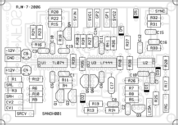
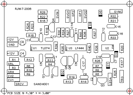
Sample And Hold With VC-Clock PCB Parts Layout (Parts Side Shown) PDF
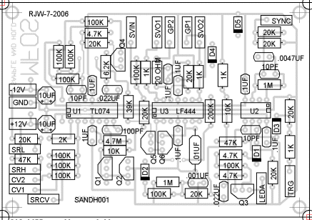
Sample And Hold With VC-Clock PCB Part Values Layout (Parts Side Shown) Larger GIF
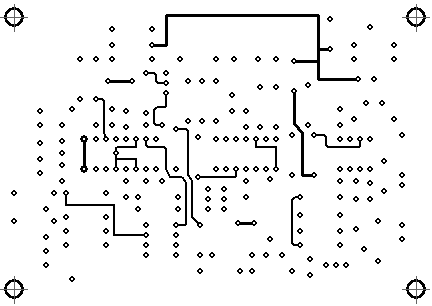
Sample And Hold With VC-Clock PCB Bottom Copper (Parts Side Shown)
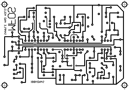
Sample And Hold With VC-Clock PCB Top Copper(Parts Side Shown)
Sample And Hold With VC-Clock PCB Top Silk Screen
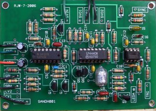
Sample And Hold With VC-Clock PCB Populated
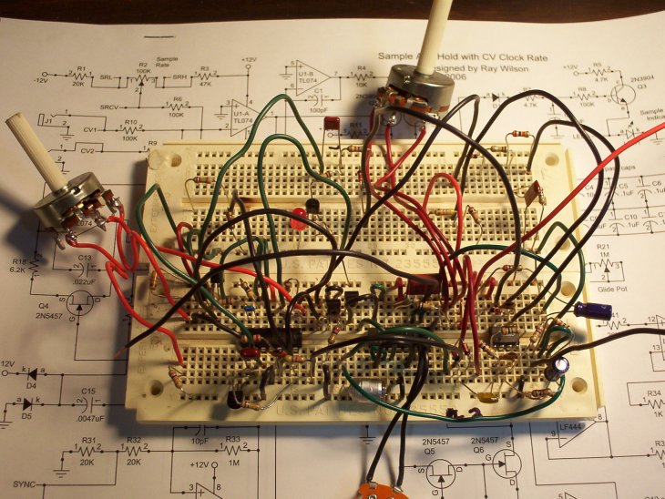
Sample And Hold With VC-Clock on the Breadboard
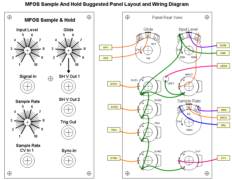
Sample And Hold With VC-Clock Front Panel and Wiring PDF
Sample And Hold With VC-Clock Project Parts List
- Using 1% metal film resistors everywhere will reduce temperature related drift.
- Where 1% metal film is specified 5% carbon comp will work but with more temperature drift.
- MPF102 or J210 can be used in place of 2N5457.
- Usually biFET amps (quads, duals, singles) can be replaced with an equivalent from another manufacturer.
- Capacitors can be film, ceramic, or silver mica.
- LM13700 subs (if applicable) (LM13600, NE5517, AU5517, NTE870).
| Qty. | Description | Value | Designators |
|---|---|---|---|
| 1 | LF444 Quad Op Amp | LF444 | U3 |
| 1 | TL074 Quad Op Amp | TL074 | U1 |
| 1 | TL082 Dual Op Amp | TL082 | U2 |
| 5 | 1N914 Sw. Diode(s) | VALUE | D4, D5, D2, D3, D1 |
| 3 | 2N3904(s) | 2N3904 | Q2, Q1, Q3 |
| 3 | 2N5457 N Channel FET | 2N5457 | Q4, Q6, Q5 |
| 1 | LED | LED | LED1 |
| 2 | Potentiometer(s) | 100K | R29, R2 |
| 1 | Potentiometer | 1M | R21 |
| 10 | Resistor 1/4 Watt 5%(s) | 100K | R9, R6, R16, R28, R23, R24, R30, R8, R13, R10 |
| 2 | Resistor 1/4 Watt 5%(s) | 10K | R4, R38 |
| 4 | Resistor 1/4 Watt 5%(s) | 1K | R36, R37, R34, R17 |
| 2 | Resistor 1/4 Watt 5%(s) | 1M | R33, R19 |
| 1 | Resistor 1/4 Watt 5% | 20 ohm | R27 |
| 1 | Resistor 1/4 Watt 5% | 200K | R40 |
| 9 | Resistor 1/4 Watt 5%(s) | 20K | R15, R31, R32, R20, R25, R14, R35, R41, R1 |
| 1 | Resistor 1/4 Watt 5% | 2K | R12 |
| 1 | Resistor 1/4 Watt 5% | 39K | R39 |
| 3 | Resistor 1/4 Watt 5%(s) | 4.7K | R22, R5, R7 |
| 1 | Resistor 1/4 Watt 5% | 4.7M | R11 |
| 2 | Resistor 1/4 Watt 5%(s) | 47K | R3, R26 |
| 1 | Resistor 1/4 Watt 5% | 6.2K | R18 |
| 1 | Ceramic Capacitor | .001uF | C8 |
| 1 | Ceramic Capacitor | .0047uF | C15 |
| 1 | Polystyrene Capacitor (low leakage) | .01uF | C17 |
| 2 | Ceramic Capacitor(s) | .022uF | C13, C2 |
| 7 | Ceramic Capacitor(s) | .1uF | C5, C6, C10, C11, C14, C7, C12 |
| 1 | Ceramic Capacitor | 100pF | C1 |
| 3 | Ceramic Capacitor(s) | 10pF | C16, C18, C3 |
| 2 | Electrolytic Capacitor(s) | 10uF | C4, C9 |
Miscellaneous
- 1/16" Thick aluminum plate for mounting the pots and switches.
- Unit is typically mounted in a synth case with other synth modules.
- Assorted hardware 1" 6-32 nuts and bolts, 1/2" #8 wood screws, etc
- Knobs for potentiometers, wire and solder.
- Digital Volt Meter and a Signal Tracer or oscilloscope for testing.