Ray Wilson authored this content while he was actively running MFOS as the founder and resident genius.
We retain the content because it reflects a valuable point of view representing that time and place.
Article by Ray Wilson
In order to use this artwork you need to print it so that the DIP IC pad holes are exactly 1/10 inch apart and 3/10 inch across. I put a lot of extra holes for any modifications you might want to make. Inspect your board to make sure none of the lands or pads are shorted. Make sure none of the lands are open. Scrape away any shorts with a Xacto knife and solder some small copper wire between any opens.Sound Lab Bottom Copper

Sound Lab Top Copper

Sound Lab Silk Screen

Important Information Pertaining to the 1V/Octave modification.
USING the 1V/Oct mod (Parts Side View)
| To implement the 1V/Octave modification insert (2) 100 ohm trimmers and (2) 475 ohm resistors in the areas indicated by the silk screened parts legend. |

NOT USING the 1V/Oct mod (Parts Side View)
| To NOT implement the 1V/Octave modification just insert (2) wire jumpers in the indicated areas. Do not install the 100 ohm trimmers or the 475 ohm resistors. |

Sound Lab Mini-Synth Parts Layout
Back to Top| I like to start with the IC sockets, then the jumpers, then the resistors, and finally caps. Essentially working from low parts to high parts will make the whole job easier. Put in about ten components at a time bending the leads to hold them in place. Now, trim the leads and solder in place, keep going until you are done. Radio shack sells a very nice "Nippy Cutter" which is excellent for trimming component leads. Remember to leave enough lead to solder to (about an 1/8 inch) and be sure that adjacent leads aren't shorted. |
LIST OF PARTS MOUNTED ON THE FRONT PANEL AND NOT THE PC BOARD
These parts are not mounted on the PC board they are mounted on either the control panel or the input/output panel.Pots: R44, R38, R29, R85, R58, R55, R48, R37, R27, R15, R11, R10, R92, R90, R19
Switches: S6, S8, S7, S15, S14, S12, S9, S10, S13, S11, S19, S5, S4,S 2, S3, S1, S18, S16, S17
Resistors: R104, R84, R52, R50, R32, R41, R94, R6, R88, R23
Diodes: D4, D3, D9, D10
Caps: C13, C22
Jacks: Gate In, Osc-2 CV, Osc-1 CV, Output
PLEASE NOTE Q7 is mounted on the board but as the schematic shows it only needs two holes because you cut the collector off.
February 2008 Parts Layout
A slight change to the layout has been made. The change allows SSM2210 matched pair transistor packages to be used for Q1/Q3 and Q2/Q4. To do this with prior boards see recommendation below. This layout began shipping in late March 2008. SSM2210 Data Sheet
May 2007 Parts Layout
To accomodate SSM2210s with May 2007 layout boards I recommend that you solder some clipped resistor leads to an 8 pin DIP socket (only 6 of the leads, pins 1,2,3 and 8,7,6) and then insert the leads into the boards and solder them. Then insert the SSM2210s into the sockets. SSM2210 Data Sheet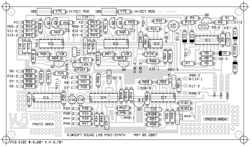
Fabian Meier's Excellent Part Value Layout
Fabian Meier of Switzerland was kind enought to share this great part value drawing for the Sound Lab. This view helps when you're stuffing the board. Instead of going back and forth between the schematic and the parts layout you can just go from here and stuff away. Click here for a PDF version. Thanks Fabian!
