Ray Wilson authored this content while he was actively running MFOS as the founder and resident genius.
We retain the content because it reflects a valuable point of view representing that time and place.
Article by Ray Wilson
Features
|
|
|
|
|
MP3 SamplesGuitar Sample Keyboard Sample (Korg X5-D) Synthesizer Sample (my modular) |
|
Introduction
This circuit automatically pans your input signal back and forth between the left channel and the right channel of your stereo amplifier. You can set it for ultra low frequency where you barely perceive the change or to faster speeds that simulate Rhodes Piano stereo tremolo or a Leslie Organ speaker. This circuit can be used with synth level signals or with audio sources like guitars, organs, or microphones. You can change the gain of the input buffer very easily by changing the value of one resistor (called out in the circuit description).Stereo Panner Page 1 PDF
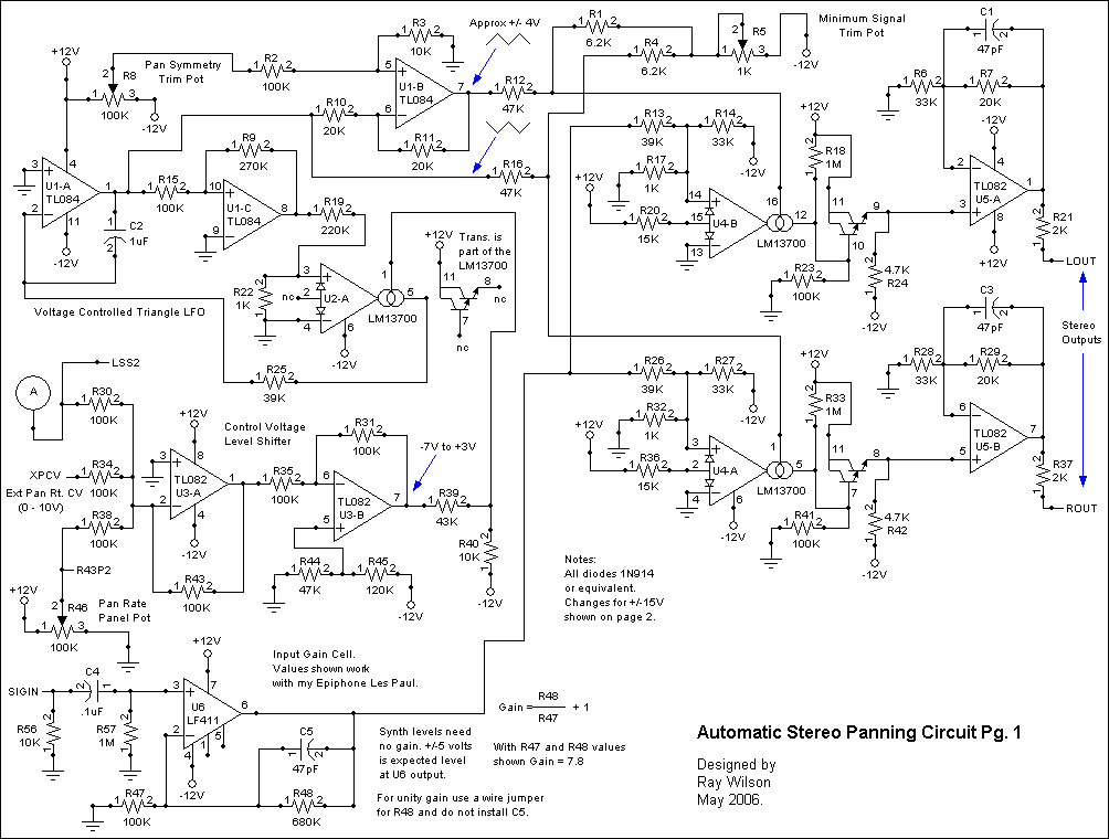
| U1 and associated components comprise the voltage controlled LFO used to modulate the amplitude of the left and right output signals. Integrator U1-A and C2 works in conjunction with
comparator U1-C and transconductance amp U2-A. U2-A controls the current that appears at the input of U1-A. Its transconductance is controlled by the control voltages summed by U3-A and level
shifted by U3-B.
When comparator output U1-C pin 8 is low (at approximately -11V) current flows into the transconductance amp and the integrator ramps up. When the ramp voltage exceeds the trip point plus hysteresis of comparator U1-C (and R15 and R9) it's output goes high (approximately +11V) and current flows out of the transconductance amp and the integrator ramps down until the negative trip point is reached and the comparator goes low. This cycle continues resulting in triangular oscillations of the voltage at the output of U1-A. U1-B is used to invert the U1-A integrator's triangle wave. Thus we have two triangle waves which are 180 degrees out of phase from one another. These signals are used to control the transconductance of the VCAs (U4-A and U4-B and associated components). The resulting output appears to float between the left and right outputs. U6 is used to buffer the input signal. The gain can be changed to suit your use. Gain formula is simply 1 + (value of R48 divided by the value of R47). If you are feeding in a high level signal like raw synth oscillators or module outputs (level of several volts) you may just want a gain of one which is accomplished by using a wire jumper for R48 and eliminating R47 and C5. Notice the changes needed to accommodate +/-15V if you use that voltage level (listed on schematic page 2). R8 is trimmed while observing both output channels on a scope while feeding in a test waveform (Suggest 1Khz 1Vpp triangle) and adjusting so that the peaks of the modulated signals of both channels are the same. R5 is trimmed while observing the same signal on both channels. Adjust R5 for the minimum desired signal level during the valleys of the amplitude modulation. If the small amount of DC offset in the output is a problem in your system you can add capacitors in series with the output current limiting resistors on both channels (suggested value 1uF). Recent observations... While recently building two of these units I discovered that I needed to reduce the value of R40 to 6.2K to achieve very very slow panning. With this value the panning may actually stop when the pan rate control is adjusted fully counter-clockwise. Also I suggest that you have the pan rate control set to about 9:00 o-clock while adjusting the high and low rates for the Leslie simulator. The pan rate will still be in effect when you use the Leslie simulator effect and can be used to adjust the low modulation rate. |
Output Amplitude Symmetry Adjust PDF
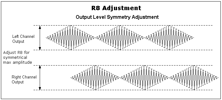
| Use R8 to adjust the maximum amplitude of the Left Output (LOUT) to match the maximum output of the Right Output (ROUT). R8 is trimmed while observing both output channels on a scope while feeding in a test waveform (Suggest 1KHZ 1VPP triangle) and adjusting so that the peaks of the modulated signals of both channels are the same amplitude. |
Minimum Amplitude Adjust PDF
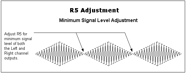
| R5 is trimmed while observing the same signal on both channels. Adjust R5 for the minimum desired signal level. You can adjust R5 so that a small amount of signal remains on at the minimum level or so that no signal remains for a small period of time. In that case the minimum signal will be 0 and the valleys will be flat (at baseline) for a small time. |
Stereo Panner Page 2 PDF
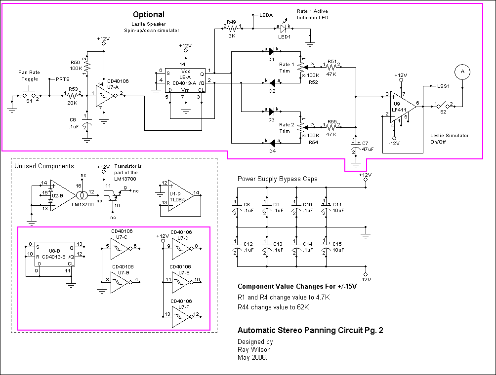
| If you don't want to use the spin-up/spin down function then do not install any of the components within the magenta boxes on the PC board (R50, R55, R54, R53, U8, R49, D3, D4, R51, R52, D1, D2, U7, S1, LED1, C7, C6, S2, U9) because they will not be needed. This circuit provides a simple mechanism to generate two adjustable voltage levels to be fed to the CV input of the panner. Momentary N.O. pushbutton S1 is debounced by U7-A and associated components. U8-A is a flip flop wired as a toggler. The state of Q and /Q change each time the button is pressed since a clean low to high transition of the output of U7-A occurs each time the button is pressed. Note that /Q is fed to the data input. When a low to high transition is presented to the clock input the level of data on the D input is propogated to the Q output. /Q is always the opposite of Q and thus the toggling functionality. The Q and /Q outputs are used to apply voltage to either R52 or R54 via diodes D1 thru D4. Trim R51 for the high Leslie rate and R55 for the low Leslie rate. That way the LED will indicate high rate. Resistors R51 and R55 in conjunction with C7 provide lag time for the change from one voltage to another which causes the stereo tremolo to increase or decrease in rate in a manner similar to the mechanical rotors on a Leslie organ speaker. U9 buffers the voltage on C7. S2 is used to connect/disconnect the Leslie simulator output voltage to/from the CV input summer (U3-A). |
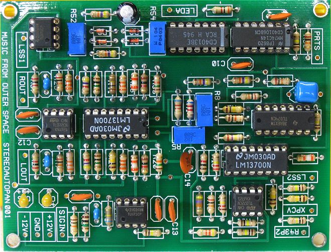
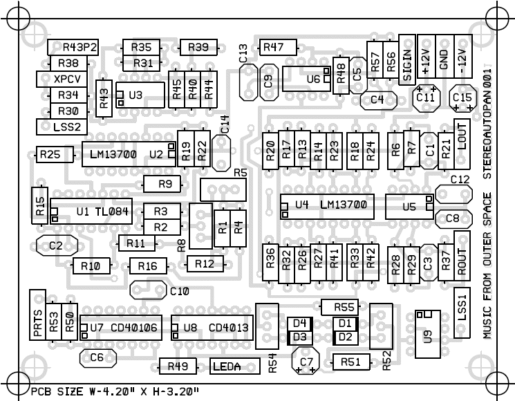
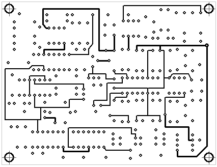
Stereo Panner PCB Parts Layout (Parts Side Shown) PDF
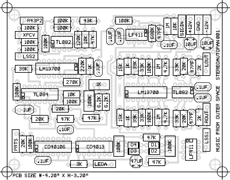
Stereo Panner PCB Parts Values (Parts Side Shown) PDF
Stereo Panner PCB Parts Layout (Parts Side Shown)
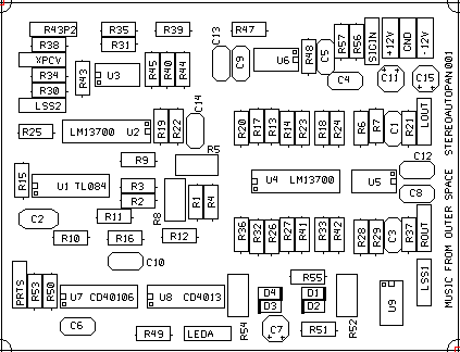
Stereo Panner PCB Bottom Copper (Parts Side Shown)
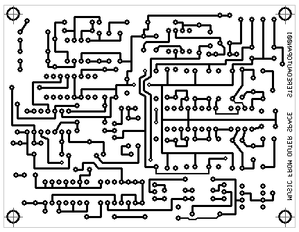
Stereo Panner PCB Top Copper(Parts Side Shown)
Stereo Panner Panel Layout Example PDF
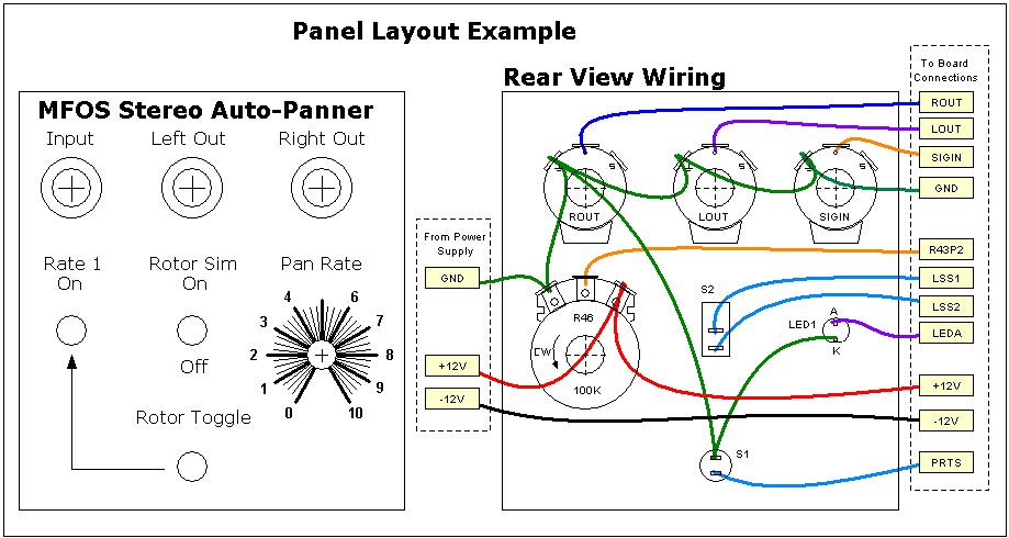
MFOS Universal Panel Layout Idea
Another Panel Example For A Dual Panner Layout (Template)
Another Panel Example For A Dual Panner Layout (Wiring)
Stereo Panner Project Parts List
| Substitutions LM13700 - LM13600, NE5517, AU5517, NTE870 TL084 - Any quad bifet (or JFET) op amp (with matching pin-out) TL082 - Any dual bifet (or JFET) op amp (with matching pin-out) LF411 - Any single bifet (or JFET) op amp (with matching pin-out) CD40106 - 74C14 (NOT HC CMOS) |
Stereo Panner Parts List
| Qty. | Description | Value | Designators |
|---|---|---|---|
| 1 | CD40106 | CD40106 | U7 |
| 1 | CD4013 Dual D Flip Flop | CD4013-A | U8 |
| 2 | LF411 Op Amp | LF411 | U6, U9 |
| 2 | LM13700 Dual gm OpAmp | LM13700 | U2, U4 |
| 2 | TL082 Dual Op Amp | TL082 | U3, U5 |
| 1 | TL084 Quad Op Amp | TL084 | U1 |
| 1 | General Purpose LED | GP-LED | LED1 |
| 4 | 1N914 Sw. Diode | 1N914 or 1N4148 | D3, D4, D1, D2 |
| 8 | Ceramic Capacitor | .1uF | C4, C8, C9, C10, C12, C13, C14, C6 |
| 1 | Ceramic Capacitor | 1uF | C2 |
| 3 | Ceramic Capacitor | 47pF | C5, C1, C3 |
| 2 | Electrolytic Capacitor | 10uF | C11, C15 |
| 1 | Electrolytic Capacitor | 47uF | C7 |
| 1 | Potentiometer | 100K | R46 |
| 3 | Trim Pot | 100K | R8, R54, R52 |
| 1 | Trim Pot | 1K | R5 |
| 12 | Resistor 1/4 Watt 5% | 100K | R15, R35, R31, R38, R43, R2, R23, R41, R34, R30, R47, R50 |
| 3 | Resistor 1/4 Watt 5% | 10K | R3, R40, R56 |
| 1 | Resistor 1/4 Watt 5% | 120K | R45 |
| 2 | Resistor 1/4 Watt 5% | 15K | R20, R36 |
| 3 | Resistor 1/4 Watt 5% | 1K | R22, R17, R32 |
| 3 | Resistor 1/4 Watt 5% | 1M | R18, R33, R57 |
| 5 | Resistor 1/4 Watt 5% | 20K | R10, R11, R29, R7, R53 |
| 1 | Resistor 1/4 Watt 5% | 220K | R19 |
| 1 | Resistor 1/4 Watt 5% | 270K | R9 |
| 2 | Resistor 1/4 Watt 5% | 2K | R37, R21 |
| 4 | Resistor 1/4 Watt 5% | 33K | R14, R27, R6, R28 |
| 3 | Resistor 1/4 Watt 5% | 39K | R26, R13, R25 |
| 1 | Resistor 1/4 Watt 5% | 3K | R49 |
| 2 | Resistor 1/4 Watt 5% | 4.7K | R24, R42 |
| 1 | Resistor 1/4 Watt 5% | 43K | R39 |
| 5 | Resistor 1/4 Watt 5% | 47K | R44, R16, R12, R55, R51 |
| 2 | Resistor 1/4 Watt 5% | 6.2K | R1, R4 |
| 1 | Resistor 1/4 Watt 5% | 680K | R48 |
| 1 | SPST PB Switch | SPST | S1 |
| 1 | SPST Switch | SPST | S2 |
Miscellaneous
- (1) 4" x 10" 1/16" thick Aluminum plate for mounting the pots and switches.
- Unit is typically mounted in a synth case with other synth modules.
- Assorted hardware 1" 6-32 nuts and bolts, 1/2" #8 wood screws, etc
- Knobs for potentiometers, wire, solder and typical assorted electronics hand tools.
- Digital Volt Meter and a Signal Tracer or oscilloscope for testing.