Ray Wilson authored this content while he was actively running MFOS as the founder and resident genius.
We retain the content because it reflects a valuable point of view representing that time and place.
Article by Ray Wilson
If you bought a prototype board these links show the necessary kludge. You need to add a 470K resistor between the -12V point at U3 pin 4 and the gate of Q11. Support docs for the prototype boards are right here:
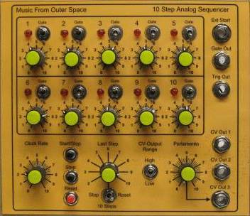
Features
IntroductionThe MFOS Ten Step Analog Sequencer is a great first sequencer project. The main idea of a sequencer is to provide an automatic means of sequentially stepping through a series of adjustable voltages to drive a VCO (or any other voltage controlled device). Additionally, gate and trigger signals are generated as the sequencer steps to each new voltage. A sequencer can control the frequency of an oscillator (or several oscillators) to produce repeating tonal patterns, or arpeggios. This sequencer design is simpler than the MFOS 16 step sequencer and has fewer steps and features. Nevertheless, it is still a fun synth-diy project. A sequencer is a mainstay of any modular analog synthesizer. |
 |
MFOS Ten Step Analog Sequencer MP3 Samples
These samples have a touch of reverb and do not use the MFOS voltage quantizer. Atonal Electronic Sequence Modulating Sequence Modulating Sequence and Keyboard Voltage External Start Demo - Keyboard trigger starts arpeggio sequence External Start Demo - Keyboard trigger starts fast arpeggio sequenceMFOS Ten Step Analog Sequencer Schematic Page 1 PDF
|
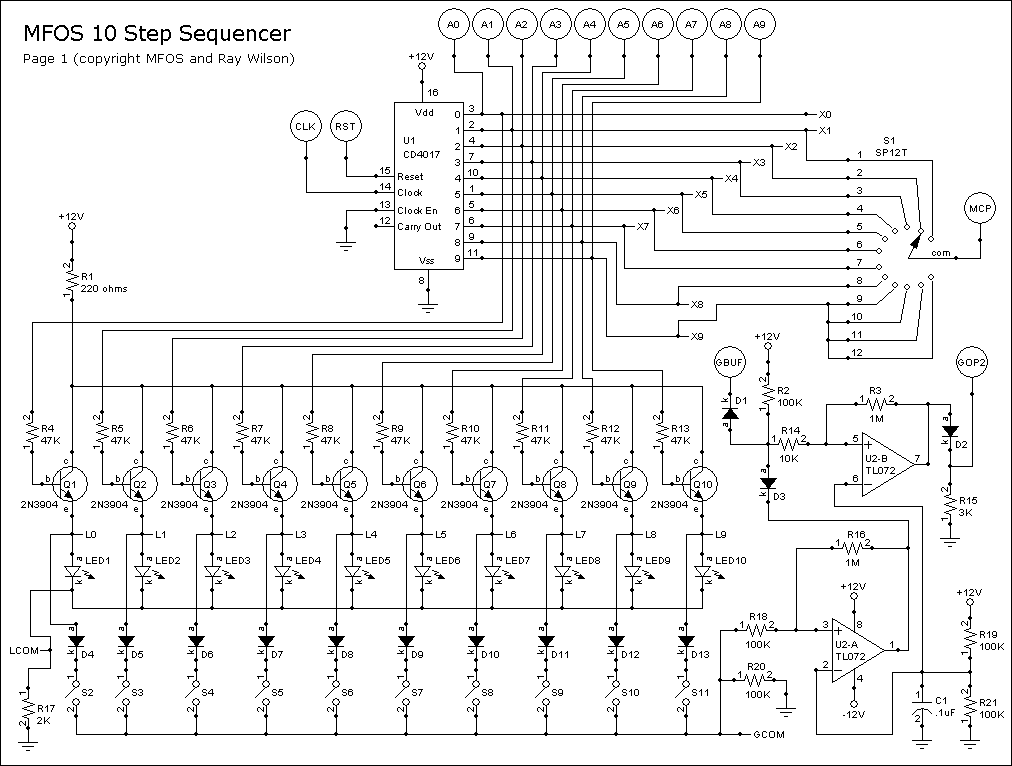
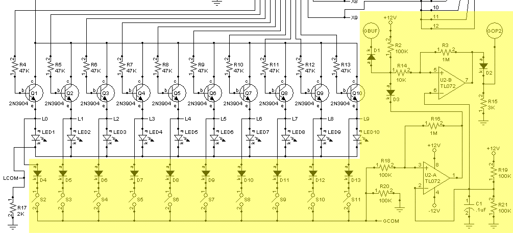
Page 1 Schematic Explanation
Page 1 shows the heart of the sequencer which is U1 (CD4017B CMOS Decade Counter with 10 Decoded Outputs). This chip has ten outputs (0 thru 9), each of which goes high sequentially (while the
others are low) when the clock input is clocked (goes from low to high) while the clock enable input is low. This circuit uses the clock and the reset inputs only. The Clock enable is tied to ground
and the Carry out is not used. The CLK circuit point and the RST circuit point both come from page two of the schematic (explained below). The circuitry on page two generates the clock pulses,
manual step pulses and reset pulses. A question I know I'll get is: "Why did you use a 12 position switch?" The answer is: "Because I often see 12 position switches for sale on surplus sites and I
rarely see 9 position switches (which is all you actually need)." As shown below you just wire the extra terminals to the last position used and you're good to go.
Operational Modes
The 0 thru 9 outputs of U1 go to: Points X0 thru X9, which connect to both the rotary switch and points A0 thru A9 (which conect to page three of the schematic (explained below) and to resistors R4
thru R13 which are connected to the bases of Q1 thru Q10. The rotary switch S1 is used to select the step at which either the reset or stop action takes place. When set to a number the functionality
is a bit different between the 'Reset' and 'Stop' functions.
In 'Reset' mode the sequencer never steps to the selected step. Thus setting the rotary switch to 4 while in reset mode will cause the sequencer to step like so: (1,2,3, 1,2,3, 1,2,3...). Setting the rotary switch to 7 while in reset mode will cause the sequencer to step like so: (1,2,3,4,5,6, 1,2,3,4,5,6, 1,2,3,4,5,6...). In 'Stop' mode the sequencer will step to the selected channel and stop. Thus setting the rotary switch to 4 while in stop mode will cause the sequencer to step like so: (1,2,3,4 stop). Setting the rotary switch to 7 while in reset mode will cause the sequencer to step like so: (1,2,3,4,5,6,7 stop). In '10 Steps' mode the sequencer steps continually (1 thru 10, 1 thru 10, 1 thru 10...).
LED Drivers
The collectors of transistors Q1 thru Q10 are all tied together and are connected to +12V via 220 ohm LED current limiting resistor R1. The emitters of transistors Q1 thru Q10 are each tied to: the
anode of it's respective channel's indicator LED (LED1 thru LED10) and the anode of it's respective channel's gate steering diode (D4 thru D13). All of the cathodes of the channel indicator LEDs are
tied together and connect to point LCOM which brings them all to ground via the 2K LED current limiting resistor R17.
Whenever an output of U1 goes high current flows through it's respective 47K resistor into the base of it's respective LED driver transistor and turns it on. Thus current flows through the respective channel's transistor collector to emitter and it's LED glows. The LEDs don't just look cool they let you know which channel is active as you set up your sequence.
Channel Gate On/Off
The cathodes of diodes D4 thu D13 are each tied to one side of it's respective channel's gate on/off switch. When a channel's gate on/off switch is turned on then when the sequencer steps to that
channel a gate and trigger are output during that step. If it is off then no gate/trigger are output during that step. When an output of U1 (CD4017B) goes from low to high it's respective transistor
turns on, applying current to the cathode of it's respective LED. This results in an approximate 9 to 10 volt drop across the LED in series with current limiting resistor R17. If a channel's gate
on/off switch is on then it's respective gate steering diode is forward biased and allows current to flow and create a voltage drop across R20. This voltage is presented to the non-inverting input
of U2-A (via R18) which acts as a comparator (1M R16 provides a bit of hysteresis). When the voltage on it's non-inverting input exceeds the voltage on it's inverting input (+6V) it's output snaps
from -12V to +12V. When the output of U2-A is high diode D3 is reverse biased. When point GBUF is high at the same time diode D1 is also reverse biased thus current through R2 causes the
non-inverting input of U2-B (also in a comparator configuration) to go high and U2-B's output snaps from -12V to +12V. Diode D2 blocks the -12V excursion so that point GOP2 only goes from ground to
+12V when U2-B goes from -12V to +12V. Op amp U2-B acts as an AND gate because it's output only goes high when both GBUF and the output U2-A are high. Point GBUF goes high everytime U1 is clocked.
It stays high for about 75% of the step time. By selectively ANDing the output of any U1 step and GBUF (via switches S2 thru S11) we provide the gate on/off per step functionality. Point GOP2
connects to page two of the schematic where the gate and trigger signals are further processed. Components R19, R21 and C1 provide the reference voltage for both comparators. |
MFOS Ten Step Analog Sequencer Schematic Page 2 PDF
|
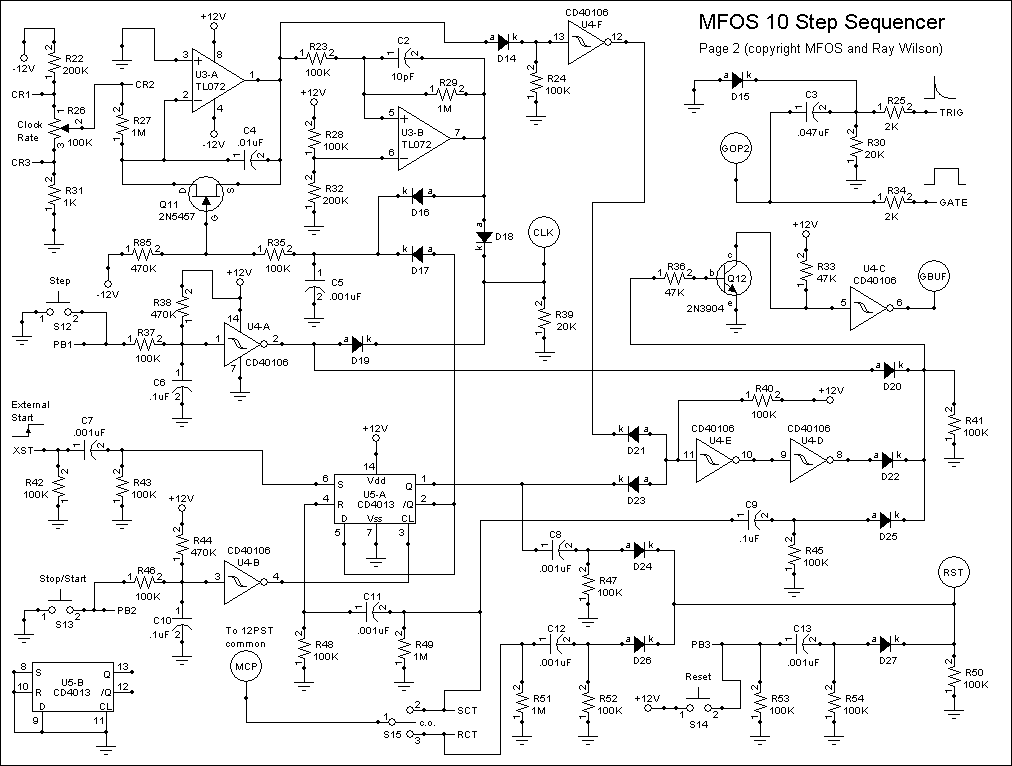
Page 2 Schematic Explanation
Page 2 shows all of the control circuitry used to start, stop, step and run the sequencer. I think it's the most interesting part of this circuit.
Gateable Clock Oscillator
In the upper left corner is the sequencer's gated clock generator. It is essentially an integrator (U3-A and associated components) followed by a comparator (U3-B and associated components). The
input to the integrator is the adjustable voltage that comes from pot R26. When R26 is adjusted so that the voltage on it's wiper is more negative the integrator ramps up faster. When R26 is
adjusted so that the voltage on it's wiper is closer to ground the integrator ramps up slower. When the voltage on the output of the integrator U3-A goes above the threshold of comparator U3-B which
is slightly above +9V dues to R29's hysteresis contribution U3-B's output shoots from -12V to +12V. This resets the comparator to ground via D16 and R35. N Channel JFET Q11's gate is held at -12V
via R85 470K resistor so when the comparator's output is low the JFET is off. But when the comparator shoots high current through forward biased diode D16 charges C5 and puts current through R35
which turns on the JFET which shorts the integrator capacitor C4 (thus resetting the integrator to ground). C5's mission is to hold a bit of charge to cause Q11 to stay on long enough to completely
discharge C4. The reset pulse from the comparator is quite narrow due to the fact that Q11 turns on so quickly and brings U3-A's output below U3-B's threshold. But that squirt of charge into C5
keeps Q11 on a bit longer and C4 is discharged nicely by Q11.
In order for the integrator/clock generator to run the NOT-Q output of D Flip Flop U5-A (pin 2) must be low. When U5-A pin 2 is high Q11 is held on (via D17) thus shorting the integrator cap and keeping U3-A's output at ground and U3-B's output low (-12V). The clock only generates pulses when the sequencer is in the 'Running' state (U5-A pin 1 Q output high).
Clock And Step
The pulses on the output of U3-B reset the comparator as well as provide the clock pulses for U1 (CD4017B CMOS Decade Counter). The positive excursions of the -12V to +12V pulses on the output of
U3-B forward bias D18 and drop voltage on R39. The CLK circuit point goes to page one of the schematic (explained above). Manual stepping is provided by the circuit of U4-A and associated
components. Normally R38 keeps C6 charged thus hold the output of U4-A low. When S12 (N.O. momentary pushbutton) is pressed C6 discharges to about 2V through R37. The filtering provided by the RC
and the schmitt trigger action of the CD40106 combine to debounce the pushbutton press into a clean step. When the button is released the voltage on C6 charges to 12V again and the output of U4-A
goes cleanly low. The output of U4-A is fed via D19 to drop voltage on R39. In this manner the clock pulses and the step pulses are ORed and either of them can advance the CD4017B counter U1.
Gate Generation
D14 protects U4-F from seeing any negative excursions of the output of U3-A. During normal operation U3-A's output should stay between ground and +12V but when the unit is turned on or off a
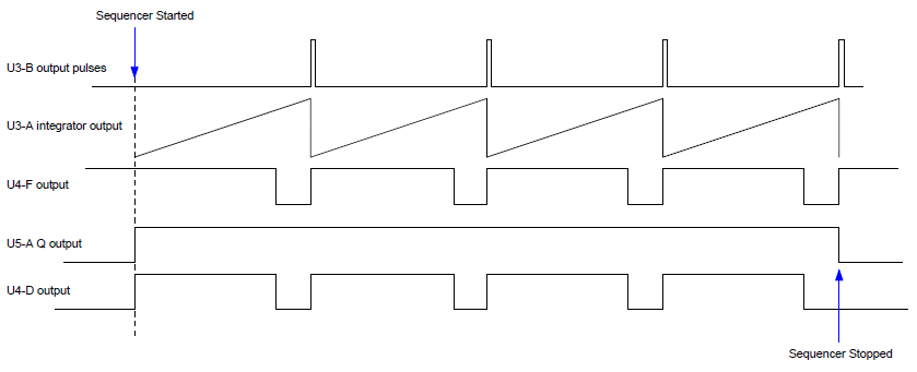
momentary negative level is possible. While U3-A's output is ramping up the output of inverting schmitt trigger U4-F is high until U3-A's output voltage exceeds U4-F's threshold (approximately 8V).
After U3-A's output voltage exceeds U4-F's threshold U4-F's output goes low. This arrangement causes the output of U4-F to go high at the same time a clock pulse it emitted (see diagram below).
Since the output of U4-F is high whenever the integrator's output is reset it is necessary to AND it with the Q output of U5-A CD4013B flip flop (pin 1). This is done so that when the sequencer is in the stopped state (Q output of U5-A CD4013B flip flop low) the gate output is low. Components D21, D23 and R40 in conjunction with U4-E and U4-D comprise the AND gate used for generating the gate pulses. The cathodes of D21 and D23 are the inputs to the and gate. When either input is low, pin 11 of U4-E is held low. When both inputs are held high pin 11 of U4-E is pulled high via R40 and U4-E's output is low. U4-D inverts U4-E's output and thus U4-D's output goes high. This composite AND gate's output is one of three things that can cause a gate output. The other two are: the step pulse generator (output of U4-A), and the output of the U1 channel that causes the sequencer to stop when in stop mode. The selected U1 output is fed via S1's common to point MCP which connects to S15 Sequencer Mode select switch. When S15 pin 1 is closed to pin 2 the rising edge of the terminating channel's output pulse is dropped across R45 via C9. D25 permits the pulse to be dropped on R41. This last thing is done so that you get a short gate on the last output when in stop mode. Otherwise you would not get one since the last step in stop mode resets U5-A and stops the clock. The three ORed gate sources all drop voltage on R41 when they are active (high). Anytime there is a high voltage (+12V) on R41 current through R36 turns transistor Q12 on which brings pin 5 of U4-C low. U4-C inverts it's input and outputs a high at point GBUF. GBUF is used on schematic page 1 and works in conjunction with the channel gate on/off circuitry. Point GOP2 comes from schematic page 1 and is the gate output. The front edge of the gate signal is fed via C3 and dropped on R30 and become the trigger output. R25 and R34 protect the gate circuitry from shorts to ground or other voltages. If you don't need or want selective gate on/off capability you can connect point GBUF to point GOP2 directly and eliminate the following components from the PCB board and eliminate the additional front panel wiring: (R20, R19, R21, C1, R3, D1, D3, D2, R2, R15, R14, R16, U2, R18, D4, S2, D5,D6, S4, D7, S5, D8, S6, D9, S7, D10, S8, D11, S9, D12,S10, S11, S3, D13). In this configuration a gate will be generated at every step all the time. The front panel wiring will be simpler but the sequencer will lack a pretty cool feature.
Components to eliminate if Selective Gate On/Off function is not desired.
Stop/Start
S13 (N.O. momentary push button) in conjunction with R46, R44, C10 and U4-B provides the pulse needed to toggle U5-A CD4013B flip flop. When NOT-Q is tied to the D input of a D flip flop each time
the CL (clock input) is brought high the Q and NOT-Q outputs toggle (i.e. Q goes high and NOT-Q goes low or visa versa). Pressing S13 causes a clean low to high transition to be applied to the CL
(clock) input of U5-A. Releasing S13 causes a clean transition from high to low. Thus the state of the sequencer is toggled between 'Running' (Q output high) and 'Stopped' (Q output low).
Last Step Stop Mode
When you are in 'Last Step Stop' mode (rotary switch set to 5 e.g.) and U5-A Q (pin 1) is low and you press the Start/Stop button the following occurs. U5-A Q (pin 1) goes high driving a pulse
through C8 and D24 which resets U1 CD4017B, simultaneously the gate output goes high and a trigger is emitted (assuming the channel 1 gate on/off switch is on). The voltage for step one is output
from the CV outputs for a clock period (as the integrator ramps up) and then the clock starts emitting pulses. The counter counts ahead on each clock output until it steps to channel 5. At that
point the rising edge of channel 5 (fed via S1 and S15) drives a pulse through C11 which resets U5-A and drives a pulse through C9 (last step pseudo gate). The sequencer stops at step 5 and step 5's
voltage is output from the CV outputs until the sequencer is started again.
Last Step Reset Mode
When you are in 'Last Step Reset' mode (rotary switch set to 5 e.g.) and U5-A Q (pin 1) is low and you press the Start/Stop button the following occurs. U5-A Q (pin 1) goes high driving a pulse
through C8 and D24 which resets U1 CD4017B, simultaneously the gate output goes high and a trigger is emitted (assuming the channel 1 gate on/off switch is on). The voltage for step one is output
from the CV outputs for a clock period (as the integrator ramps up) and then the clock starts emitting pulses. The counter counts ahead on each clock output until it steps to channel 5. At that
point the rising edge of channel 5 (fed via S1 and S15) drives a pulse through C12 which resets U1 to step 1 and the cycle repeats until the sequencer is put into 'Stopped' mode by pressing
Start/Stop. The voltage from step 5 is never output because the reset to 1 occurs as we step to step 5.
External Start
A fast rising edge (keyboard gate etc.) fed into the External Start input (XST) can be used to put the sequencer into 'Running' state. It only has an effect if the sequencer is in 'Stopped' state.
Applying an external start pulse in 'Running' state has no effect.
Reset Button
S14 applies a positive pulse to the RST circuit point when pressed. It is not debounced because it is of short duration and only has to cause U1 CD4017B to reset.
|
MFOS Ten Step Analog Sequencer Schematic Page 3 PDF
|
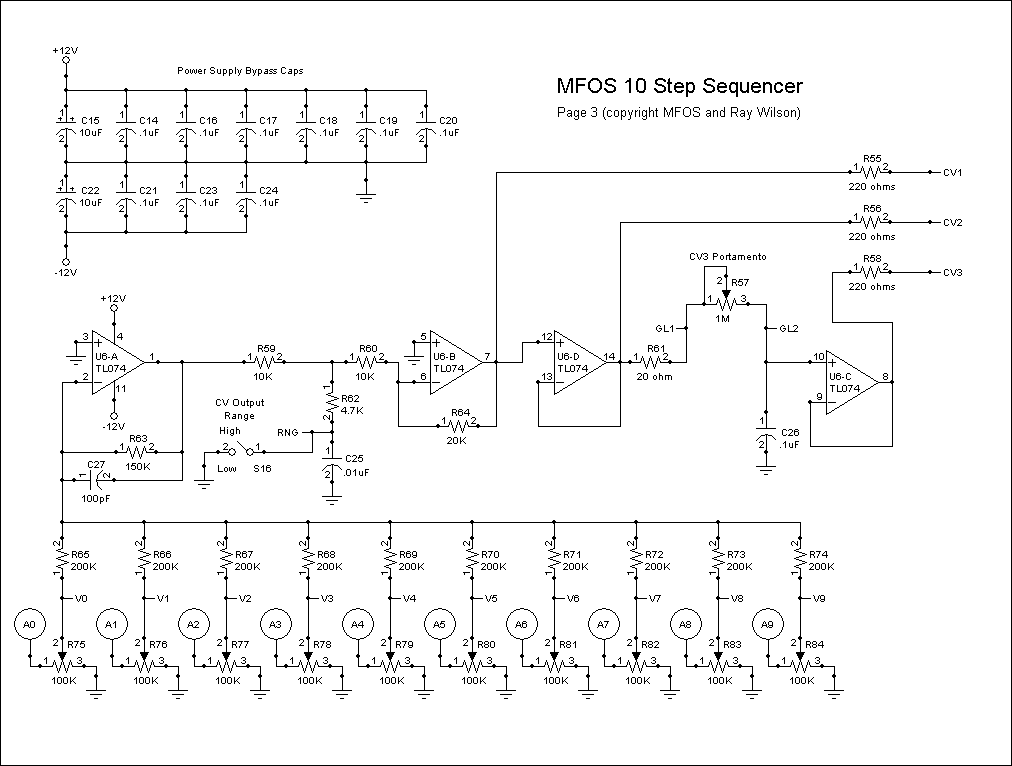
Page 3 Schematic Explanation
Page 3 shows the control voltage output circuitry. Points A0 thru A9 connect to the outputs of U1 (CD4017B CMOS Decade Counter with 10 Decoded Outputs). As each output goes high in turn it drops V+
across R75 thru R74 sequentially. Each of these pots (R75 thru R74) is wired as a variable voltage divider. When each pot is energized (i.e. it's corresponding A[n] is brought high) the voltage
appearing on it's wiper is fed to inverting voltage summer U6-A via a 200K resistor (R65 thru R74). U6-A's gain is .75 so with a +/-12V volt supply you get 0 to -9 volts at it's output as you adjust
any pot from ground to fully clockwise. We want the voltage to go from 0 to +9V so we flip it over by feeding the output of U6-A to inverting buffer U6-B.
CV Output Range switch
U6-B's output voltage will be 0 to +9V when CV Output Range switch S16 is open and 0 to about +5V when S16 is closed bringing shunting resistor R62 to ground. C25's purpose is to quiet any noise on
the wire from switch S16 when S16 is open. The outputs of U6-B and U6D are fed to the CV1 and CV2 jacks respectively.
CV3 Portamento
The output of U6-D is also connected via R61 and R57 to high impedance unity follower U6-C's non-inverting input. R57 and C26 provide adjustable lag (glide or portamento) between step voltages
appearing at the CV3 output. All outputs are protected from shorts to ground and other voltages by 220 ohm resistors.
Bypass caps
The capacitors in the upper left corner are power supply bypass caps. Every IC has one or two depending on it's supply requirements. |
| Approx. Current Consumption | |
| +12V | 30mA |
| -12V | 30mA |
| +15V | 32mA |
| -15V | 32mA |
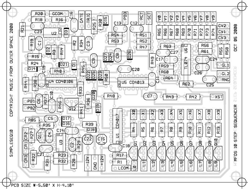
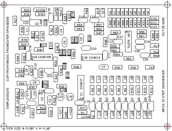
MFOS Ten Step Analog Sequencer PCB Parts Layout (Parts Side Shown) PDF
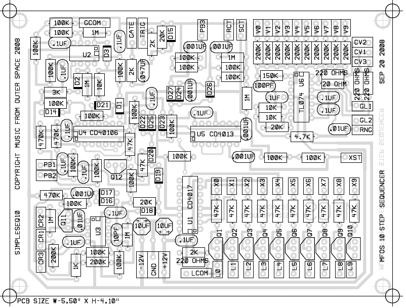
MFOS Ten Step Analog Sequencer PCB Parts Values (Parts Side Shown) PDF
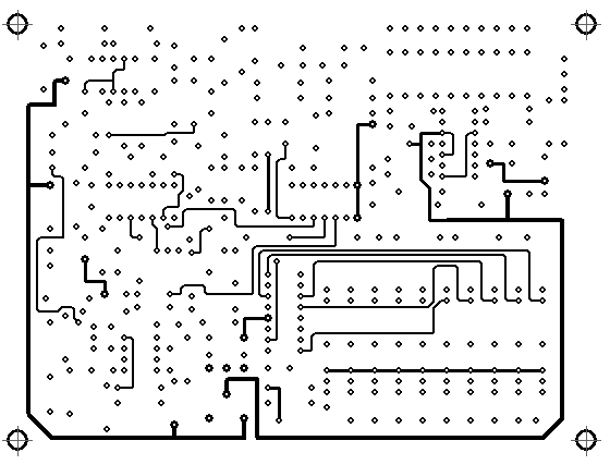
MFOS Ten Step Analog Sequencer PCB Bottom Copper (Parts Side Shown)
MFOS Ten Step Analog Sequencer PCB Top Copper(Parts Side Shown)
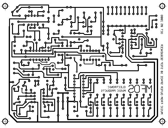
MFOS Ten Step Analog Sequencer PCB Top Silk Screen
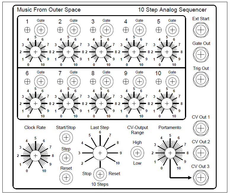
MFOS Ten Step Analog Sequencer Front Panel PDF
Front Panels contributed by other builders
Please bear in mind that if you use another front panel design that the panel wiring diagrams I provide will not apply. You will be on your own with the panel wiring. I suggest that you make your own panel wiring drawing and carefully transpose the connection information. Good wiring.
 Click image to download a larger file. |
Kristaps Boris did this nice black with white details layout. Click image to download a larger file. |
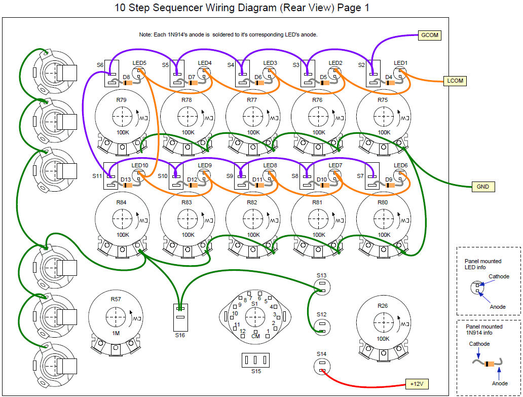
MFOS Ten Step Analog Sequencer Panel Wiring Page 1 PDF
I show the wiring in two stages. Run these wires first and then move on to the second diagram.
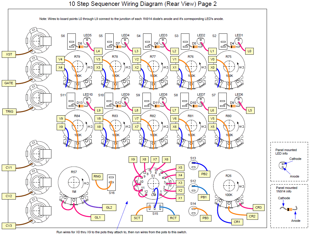
MFOS Ten Step Analog Sequencer Panel Wiring Page 2 PDF
Now run all ofthese wires between the panel and the board. I suggest that you run the wires from the rotary switch to the pot connections that go to the same point. Don't fill the pot solder lug with solder so you can still attach the wire that goes to the PC board to it.
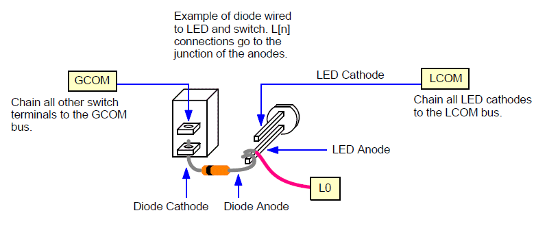
MFOS Ten Step Analog Sequencer LED and Diode To Switch Wiring Closeup PDF
Wiring these panel components takes skill and patience but there aren't that many to do (just 10 sets of LED/diode combos). So take your time and don't over stress the leads of any of the LEDs or diodes. Use small gauge wire to make this easier.
MFOS Ten Step Analog Sequencer Project Parts List
| Qty. | Description | Value | Designators |
|---|---|---|---|
| 1 | CD40106 | CD40106 | U4 |
| 1 | CD4013 Dual D Flip Flop A | CD4013 | U5 |
| 1 | CD4017 Decade Counter Decoder | CD4017 | U1 |
| 2 | TL072 Dual Op Amp(s) | TL072 | U2, U3 |
| 1 | TL074 Quad Op Amp | TL074 | U6 |
| 11 | 2N3904(s) | 2N3904 | Q1, Q2, Q3, Q4, Q5, Q6, Q7, Q8, Q9, Q10, Q12 |
| 1 | 2N5457 N Channel JFET | 2N5457 | Q11 |
| 10 | LED(s) | LED | LED1, LED5, LED7, LED8, LED9, LED10, LED6, LED4, LED3, LED2 |
| 27 | 1N914 Sw. Diode(s) | VALUE | D4, D5, D6, D7, D8, D9, D10, D11, D12, D13, D1, D3, D2, D16, D17, D19, D22, D20, D15, D18, D25, D27, D26, D24, D14, D21, D23 |
| 6 | Capacitor Ceramic(s) | .001uF | C7, C5, C11, C13, C12, C8 |
| 2 | Capacitor Ceramic(s) | .01uF | C4, C25 |
| 1 | Capacitor Ceramic | .047uF | C3 |
| 14 | Capacitor Ceramic(s) | .1uF | C1, C6, C10, C9, C26, C14, C16, C17, C18, C19, C20, C21, C23, C24 |
| 1 | Capacitor Ceramic | 100pF | C27 |
| 1 | Capacitor Ceramic | 10pF | C2 |
| 2 | Capacitor Electrolytic(s) | 10uF | C15, C22 |
| 11 | Linear Taper Potentiometer(s) | 100K | R26, R75, R76, R77, R78, R79, R80, R81, R82, R83, R84 |
| 1 | Audio Taper Potentiometer | 1M | R57 |
| 5 | Resistor 1/4 Watt 1%(s) | 100K | R20, R19, R21, R2, R18 |
| 3 | Resistor 1/4 Watt 1%(s) | 10K | R14, R59, R60 |
| 1 | Resistor 1/4 Watt 1% | 150K | R63 |
| 2 | Resistor 1/4 Watt 1%(s) | 1M | R3, R16 |
| 1 | Resistor 1/4 Watt 1% | 20 ohm | R61 |
| 10 | Resistor 1/4 Watt 1%(s) | 200K | R67, R68, R69, R70, R71, R72, R73, R74, R65, R66 |
| 1 | Resistor 1/4 Watt 1% | 20K | R64 |
| 4 | Resistor 1/4 Watt 1%(s) | 220 ohms | R1, R58, R56, R55 |
| 1 | Resistor 1/4 Watt 1% | 2K | R17 |
| 1 | Resistor 1/4 Watt 1% | 3K | R15 |
| 1 | Resistor 1/4 Watt 1% | 4.7K | R62 |
| 10 | Resistor 1/4 Watt 1%(s) | 47K | R5, R6, R7, R8, R9, R10, R11, R12, R4, R13 |
| 17 | Resistor 1/4 Watt 5%(s) | 100K | R23, R28, R41, R43, R42, R37, R46, R48, R45, R52, R53, R54, R50, R47, R24, R40, R35 |
| 1 | Resistor 1/4 Watt 5% | 1K | R31 |
| 4 | Resistor 1/4 Watt 5%(s) | 1M | R27, R29, R49, R51 |
| 2 | Resistor 1/4 Watt 5%(s) | 200K | R22, R32 |
| 2 | Resistor 1/4 Watt 5%(s) | 20K | R30, R39 |
| 2 | Resistor 1/4 Watt 5%(s) | 2K | R25, R34 |
| 3 | Resistor 1/4 Watt 5%(s) | 470K | R44, R38, R85 |
| 2 | Resistor 1/4 Watt 5%(s) | 47K | R36, R33 |
| 1 | 12 Pole Rotary Switch (non-shorting) | SP12T | S1 |
| 1 | SPDT Center Off Switch | SPDT | S15 |
| 3 | SPST N.O. Momentary PB Switch(s) | SPST | S12, S13, S14 |
| 11 | SPST Switch(s) | SPST | S2, S4, S5, S6, S7, S8, S9, S10, S11, S3, S16 |
Miscellaneous
- 1/16" Thick aluminum plate for mounting the pots and switches.
- Unit is typically mounted in a synth case with other synth modules.
- Assorted hardware 1" 6-32 nuts and bolts, 1/2" #8 wood screws, etc
- Knobs for potentiometers, wire and solder.
- Digital Volt Meter and a Signal Tracer or oscilloscope for testing.