Ray Wilson authored this content while he was actively running MFOS as the founder and resident genius.
We retain the content because it reflects a valuable point of view representing that time and place.
Article by Ray Wilson
Features
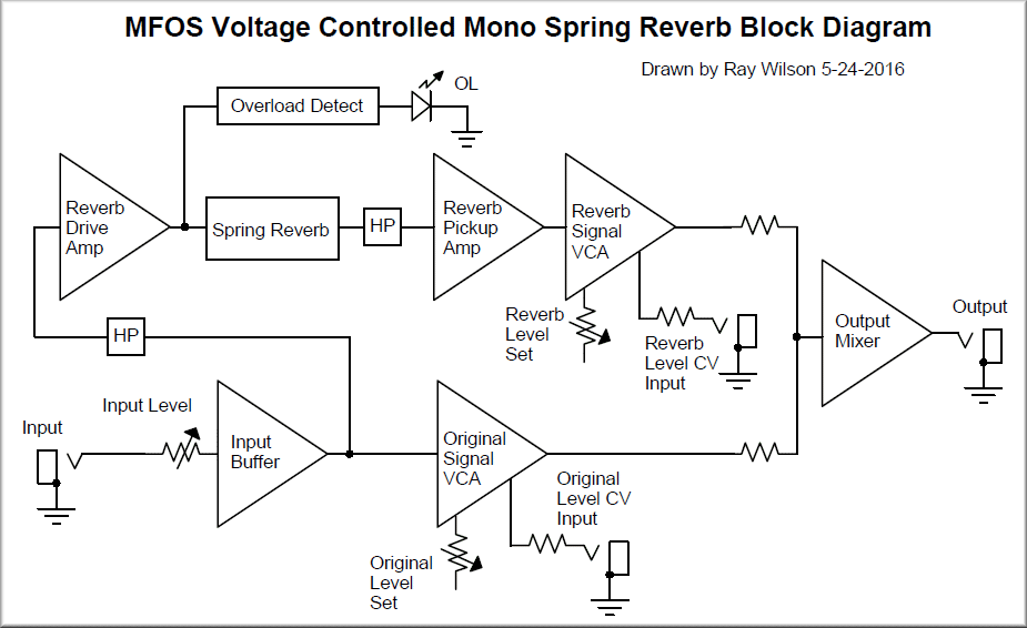
- Voltage controlled reverb level
- Voltage controlled original level
Info
- PC Board Supports One Reverb Tank
IntroductionAnalog spring reverbs have been around since the turn of the 20th century. They have changed in form and implementation but the reverberation and decay of the spring has caught the attention of many a designer. They are fairly dark in nature and severely distort the signal as it rides along the spring mixed with signals that are already coming and going along the vibrating spring. In the end it definitely give the impression of a virtual space which is why they have remained popular for close to 100 years. This design adds two simple features to the simple spring reverb. Voltage control of the original signal and voltage control of the reverb signal. This gives you several options for bringing dry and wet under voltage control. Simple I know but combined with your other modules and mixers I think you'll like this. I hope to get that second reverb into that plate when I get a charge of energy. I'm going to be focusing on healing 100%. I hope you've found and continue to find cool and challenging projects here at MFOS. namaste.
|
|
Block Diagram
Schematics
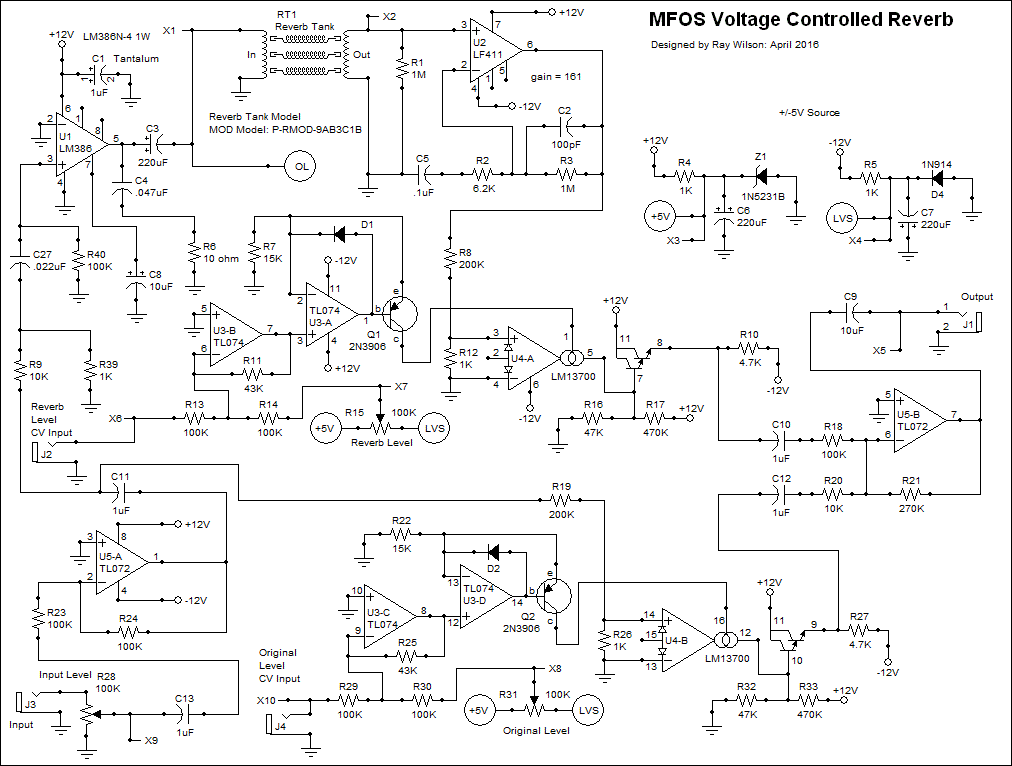
Schematic Page 1
View as PDFMuch easier to print the schem and read along. The input is applied via J3 (input jack). Attenuation of the input signal is controlled by R28 100K potentiometer. The wiper of R28 feeds 1uF non-polarized cap C13 in series with R23 which is connected to the inverting input of inverting buffer amp U5-A. The 100K feedback resistor R24 sets the gain for the input buffer to 1. The output of the input buffer drives both the reverb tank driver amp U1 (LM38N4 1W amp) and the Original Level VCA. The signal going to the reverb tank driver amp U1 is attenuated via R9 and R39 and then passively high pass filtered via C27 .022uF ceramic cap dropping the passed signal onto R40 100K resistor. If you want to attenuate more low frequency signals (which darken the reverb) you can either decrease the value of R40 (80K, 47K, etc) or decrease the value of C27 (from .022uF to .01uF for instance). The LM386N4 is set to its minimum gain of 20 and drives the reverb tank with about 1 watt of power. C1 1uF tantalum is to stabilize the chip's supply voltage. Capacitor C4 (.047uF) and resistor R6 (10 ohm) stabilize the output of the amplifier. Cap C3 (220uF) couples the output of U1 to both the reverb tank and to point OL (explained later on page 2).
The signal impressed onto the input side of the spring is picked up at the other end by the circuit of U2 and associated components. I used the LF411 op amp because it is a low noise amplifier and we ask it to deliver a gain of 160. A noisy amp just wouldn't do. If you have a lower noise op amp sub in mind, use it as long as it can run on +/-12V power. We essentially drop the output of the reverb onto a grounded 1M resistor connected to the non-inverting input of U2 (pin 3). We set the gain for the amp via R3 1M and R2 6.2K to 160 maximum. C5 acts as a high pass filter because at lower frequencies the capacitive reactance of C5 is high thus lowering the gain of low frequency signals. However as the frequencies fed into opamp U2 rise they face less and less capacitive reactance and the gain tops out at 160 once the frequency gets to about 50 hz or so. The other advantage of connecting C5 (.1uF ceramic cap) in series with gain set resistor R2 (6.2K) is that the DC gain is 1 which keeps the opamp's offset from getting amplified. If you want to attenuate more low frequency signals in the recovery amp decrease C5 (.068uF, .047uF, etc.)
The output of U2 feeds the reverb level VCA. Both of the VCAs used in the circuit are identical and the astute observer will see that I copied them straight out of the ECHOFXXX (why reinvent the wheel). U3-A and U3-B comprise a voltage to current convertor which is used to drive the LM13700's bias pin. The attenuated signal at the non-inverting input of U4-A (LM13600 or Lm13700) is multiplied by the control current applied to the bias pin (U4-A pin 1). We use the LM13600's built in darlington pair to buffer the output of the VCA. The 1/4 watt resistors R16 (47K) and R17 (470K) bias the output. The output is picked off at pin 8 which is dropped on 4.7K resistor R10. The original level VCS functions in the same manner. The output of both VCAs go to the inputs (via C10 and C12) of output mixer U5-B and associated components. This is a simple inverting mixer that applies a gain of one to the reverb level VCA's channel and a gain of 10 for the original level VCA's gain. U5-B's output is cap coupled (via non-polarized 10uf C9) to J1, the output jack.
Two voltage sources are in the upper right corner. One is +5V and the other is -600mV. These two voltages are used to set the initial levels of the reverb and original level signals. R15 (reverb level) applies a voltage to the input of current convertor (U3-C and U3-D and associated components) via 100K resistor R14. As more voltage is applied more current is fed to U4-A's bias pin (pin 1). The reverb VCA is off when the Reverb Level knob is fully CCW and fully on when it is fully CW. The same info applies to the other VCA and R31 (Original Level).
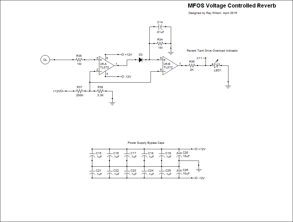
Schematic Page 2
View as PDFU1 can drive the reverb tank faithfully over a wide frequency range but at fairly low amplitude. I find that there is more distortion at low frequencies than at high ones. In any case I have been very conservative regarding the OL indicator which indicates an overlod when the voltage fed to the reverb drive coil is above about .4V PP. You can ignore the OL indicator if you like and nothing bad will happen but the low frequency signals being fed to the reverb drive coil may be severely distored. As I indicated above you can change the high pass filter driving the LM386N4 to cut off more low frequencies if desired.
U6-A is wired as a comparator and circuit point OL from page one connects to it's non-inverting input via 1M resistor R35. The threshold voltage level connected to the inverting input is pretty low, about .2 volts. Thus when the PP level going to the reverb coil drive amp is greater than about .4V the output of U6-A goes from -10V to about +10V. These excursions can be so brief that we need to stretch them which is exactly what we do with comparator U6-B. When the output of U6-A shoots high (-10V to +10V) D3 is forward biased and C14 becomes charged to U6-A's output voltage - about 600mV, this is well above the .2V threshold applied to its inverting input. When D3 conducts C14 is charged and must discharge through 1M resistor R34 to below its threshold voltage which does give enough time to catch the LED come on. So - can you run with the led coming on briefly - yes. Can you run with the LED pegged yes - but expect distortion.
And finally, as usual a raft of decoupling caps to keep the unit's power clean.
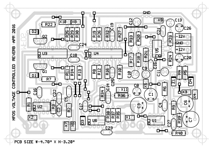
PC Board Information
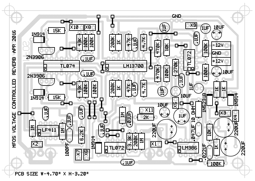
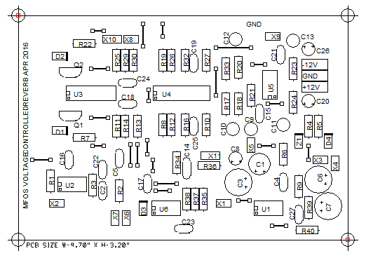
Parts Layout With Component Designators
- This is a single sided board that you can make at home.
- This view shows the designators useful when trouble shooting.
- All jumper indicators must be shorted with number 22 AWG solid wire or equivalent.
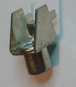
Suggested PC Mount RCA Jack
It is important to minimize noise and EMI from getting into your reverb drive or recovery circuit which is why RCA jacks are mounted directly to the PC connections they serve. These PC mount connectors are fairly generic. Drown them in solder to fill the voids of the drill holes. I got mine from All Electronics CAT# RCJ-5G at All Electronics
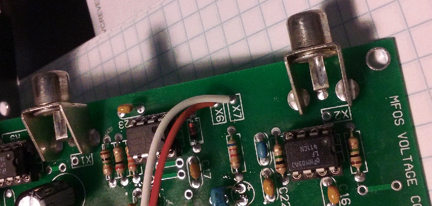
Soldered PC Mount RCA Jacks
Drown them in solder to fill the voids of the drill holes. I got mine from All Electronics CAT# RCJ-5G at All Electronics
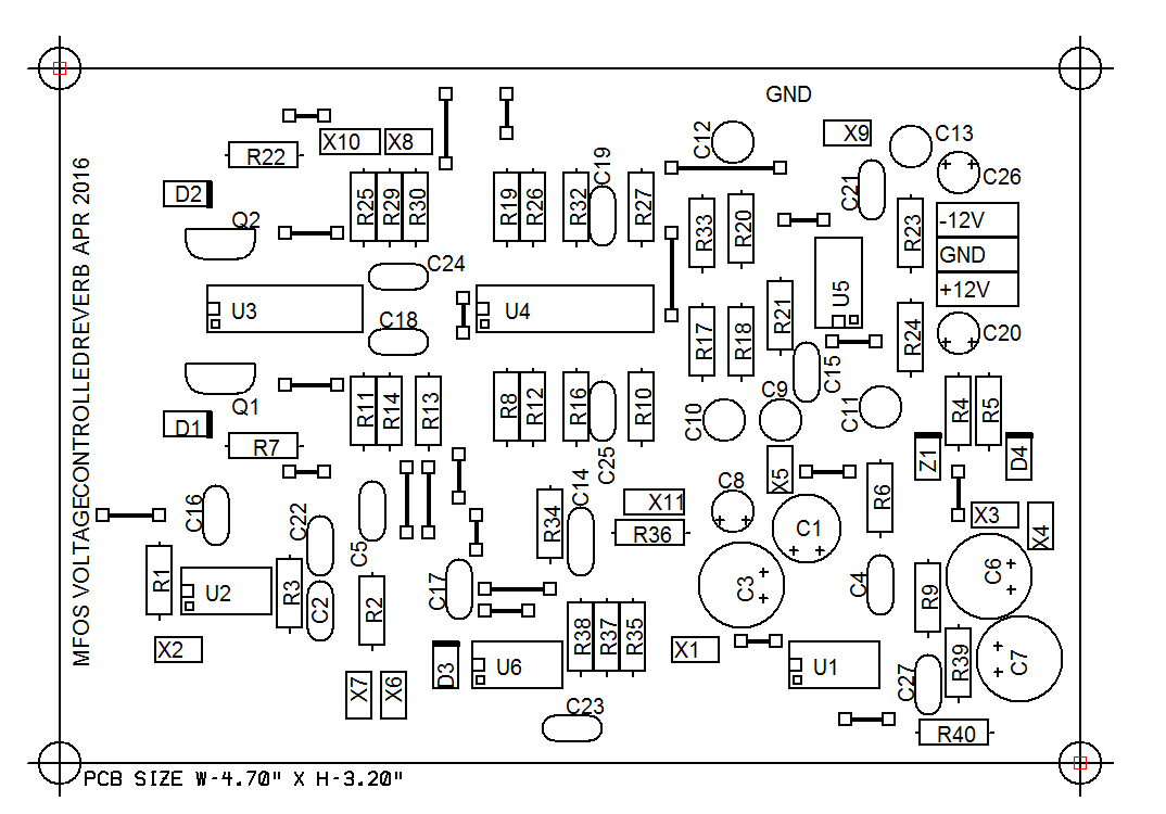
Parts Layout With Component Values
- This is a single sided board that you can make at home.
- This view shows the component values useful when populating the PC board.
- All jumper indicators must be shorted with number 22 AWG solid wire or equivalent.
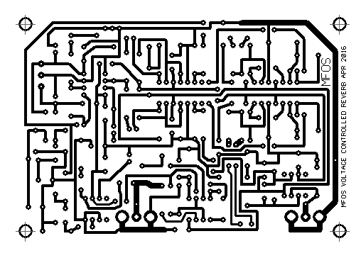
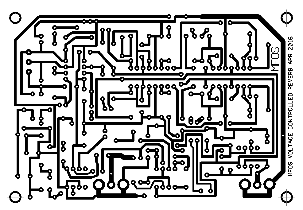
Bottom Copper X1
This PC layout is as viewed from the BOTTOM of the PC board.
Silk Screen X1
This PC silk layout is as viewed from the TOP of the PC board.
Bottom Copper X2
This PC layout is as viewed from the BOTTOM of the PC board.
Silk Screen X2
This PC silk layout is as viewed from the TOP of the PC board.
Front Panel Information
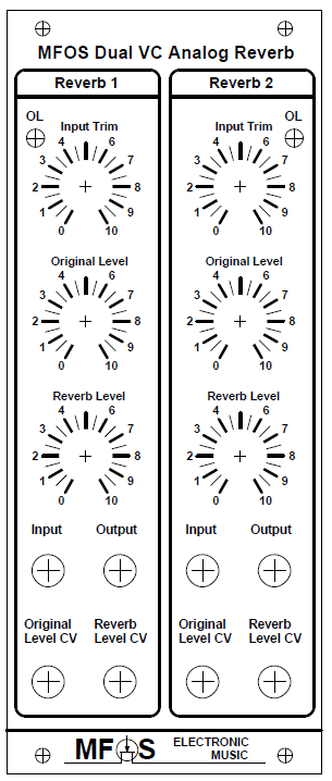
Suggested Front Panel Layout
View as PDFObvious I know but I would just use the 1U size if you only want one unit. Both reverbs get wired identically as shown.
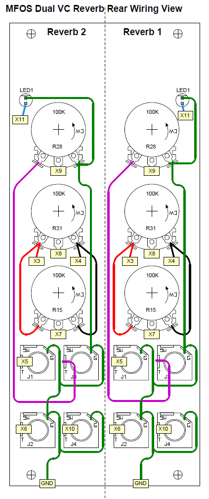
Suggested Front Panel Wiring Diagram
View as PDFI always wire the panel interconnections first and then wire the panel to the PC board. Tack solder connections when you know you'll need another wire to go to the panel if multiple wires converge at a terminal. Also use the shortest wire runs necessary the diagram uses longer than normal wires for clarity. I used coax from the input jack to the PC board to minimize EMI.
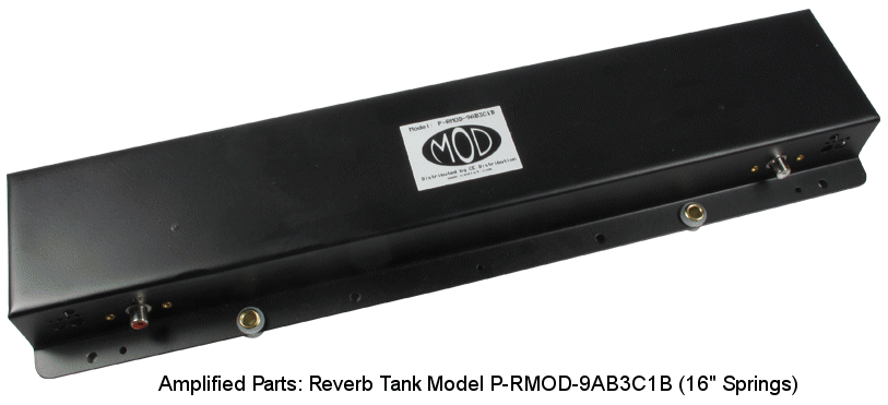
Suggested MOD Reverb Tank
I got mine from Amplified Parts P-RMOD-9AB3C1B at Amplified Parts
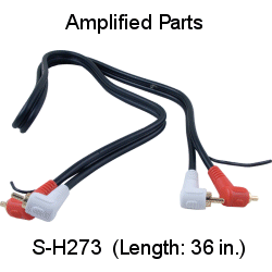
Suggested Board to Reverb Tank Cable
It is very important to keep EMI out of your reverb. The cable used to connect the reverb to the PC board has two separate RCA cables for connecting "in" and "out" on the reverb tank. I got mine from Amplified Parts S-H273 (Len.36") at Amplified Parts
MFOS Voltage Controlled Analog Spring Reverb Module
Component Notes
All cap voltages should be 25V or more. All resistors are 1/4W 5% (1% will work fine). MFOS PC boards use dual inline IC packages. MFOS PC boards usually use 5mm (0.2") cap lead spacing unless it is obvious from the board's legend that it should be larger or smaller. I often specify axial leads for any caps mounted on the front panel but you can use radial as well by adding some wire to the leads.
| Qty. | Description | Value | Designators |
|---|---|---|---|
| 1 | LF411 Op Amp | LF411 | U2 |
| 1 | LM13700 Dual gm OpAmp | LM13700 | U4 |
| 1 | LM386 Low Voltage Audio Power Amp | LM386 | U1 |
| 2 | TL072 Dual Op Amp | TL072 | U5, U6 |
| 1 | TL074 Quad Op Amp | TL074 | U3 |
| 2 | 2N3906 | 2N3906 | Q1, Q2 |
| 4 | 1N914 Sw. Diode | 1N914 | D1, D2, D3, D4 |
| 1 | Zener Diode 5.1V | 1N5231B | Z1 |
| 1 | LED | LED | LED1 |
| 3 | Linear Taper Potentiometer | 100K | R15, R28, R31 |
| 8 | Resistor 1/4 Watt 5% | 100K | R13, R14, R18, R23, R24, R29, R30, R40 |
| 2 | Resistor 1/4 Watt 5% | 10K | R9, R20 |
| 2 | Resistor 1/4 Watt 5% | 15K | R7, R22 |
| 5 | Resistor 1/4 Watt 5% | 1K | R4, R5, R12, R26, R39 |
| 4 | Resistor 1/4 Watt 5% | 1M | R1, R3, R34, R35 |
| 3 | Resistor 1/4 Watt 5% | 200K | R8, R19, R37 |
| 1 | Resistor 1/4 Watt 5% | 270K | R21 |
| 1 | Resistor 1/4 Watt 5% | 2K | R36 |
| 1 | Resistor 1/4 Watt 5% | 3.3K | R38 |
| 2 | Resistor 1/4 Watt 5% | 4.7K | R10, R27 |
| 2 | Resistor 1/4 Watt 5% | 43K | R11, R25 |
| 2 | Resistor 1/4 Watt 5% | 470K | R17, R33 |
| 2 | Resistor 1/4 Watt 5% | 47K | R16, R32 |
| 1 | Resistor 1/4 Watt 5% | 6.2K | R2 |
| 1 | Resistor 1/4 Watt 5% | 10 ohm | R6 |
| 1 | Reverb Tank P-RMOD-9AB3C1B | MOD Reverb Tank | RT1 (Get it at Amplified Parts) |
| 3 | Aluminum Electrolytic Capacitor | 10uF | C8, C20, C26 |
| 1 | Aluminum Electrolytic Capacitor | 220uF | C3 |
| 1 | Capacitor Aluminum Bipolar (non polarized) | 10uF | C9 |
| 4 | Capacitor Aluminum Bipolar (non polarized) | 1uF | C10, C11, C12, C13 |
| 2 | Capacitor Electrolytic | 220uF | C6, C7 |
| 1 | Capacitor Tantalum Electrolytic | 1uF | C1 |
| 1 | Ceramic Capacitor | .01uF | C14 |
| 1 | Ceramic Capacitor | .022uF | C27 |
| 1 | Ceramic Capacitor | .047uF | C4 |
| 11 | Ceramic Capacitor | .1uF | C5, C15, C16, C17, C18, C19, C21, C22, C23, C24, C25 |
| 1 | Ceramic Capacitor | 100pF | C2 |
| 4 | Jack 1/4" 2 Terminal | J1, J2, J3, J4 | |
| 1 | 36" Reverb Cable S-H273 | Get it at Amplified Parts |