Ray Wilson authored this content while he was actively running MFOS as the founder and resident genius.
We retain the content because it reflects a valuable point of view representing that time and place.
Article by Ray Wilson
Features
IntroductionThe MFOS Wave Former is a mashup of the MFOS Ten Step Sequencer and the MFOS VCO to produce a 1V/Octave tracking arbitrary waveform generator. Both a VCO PCB and a Ten Step Sequencer PCB are required for this project. To succeed with this project you need to understand the Sequencer project and the VCO project. Only the details of mashing them up to create the Wave Former are shown here. The VCO provides the clock signal for the sequencer allowing the output of the sequencer to be used as a signal source. The VCO is being operated in a higher frequency range than normal and thus it will not track as well at high frequency as it will at lower frequencies. The integrator cap has been changed from .005uF to 470pF effectively raising the VCO's range by a factor of ten. Neither PC board requires full population as shown in the drawings below. For full details of either project please see the respective project's page. 10 Step Sequencer Project - Full Details
|

|
Schematics
The schematics for both the VCO and the Ten Step Sequencer only show the components used for this project. The interconnections between the two PCBs are shown in the PCB drawings.
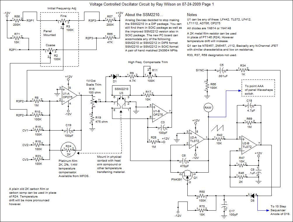
VCO Schematic (For use in Wave Former)
View as PDFFor a full description of this VCO's operation see the VCO project page (link above). The main point for this project is that we are using the output of the integrator reset comparator to clock the sequencer. The output of U2-B (pin 7) must be connected to the sequencer board at the anode of D18. Also note that the RAW ramp wave generated at the output of U2-A (pin 1) must be connected to the Waveshape switch on the panel which is shown in the panel drawings below. The VCO's integrator capacitor has been decreased in value from .005uF to 470pF to raise its frequency range by a factor of ten. The calibration procedure will be the same as used for the normal VCO except that you should work with frequencies starting at about 150Hz. (i.e 150,300,600,1200,2400,4800). At higher frequencies you can expect that the VCO will go flat. The high frequency compensation will come more into play due to the higher frequency range. However there is a wide useable range of 1V/Oct tracking operation especially at lower frequencies when using all ten steps.
The VCO's integrator reset pulses at the output of U2-B pin 7 drive the clock of the sequencer's CD4017B chip. We use the VCO's CV inputs, Coarse and Fine frequency control and the sync input of the VCO. When syncing the the output of the Wave Former does not sound like the VCO does when synced but instead the frequency of the Wave Former jumps up in steps providing a very cool effect.
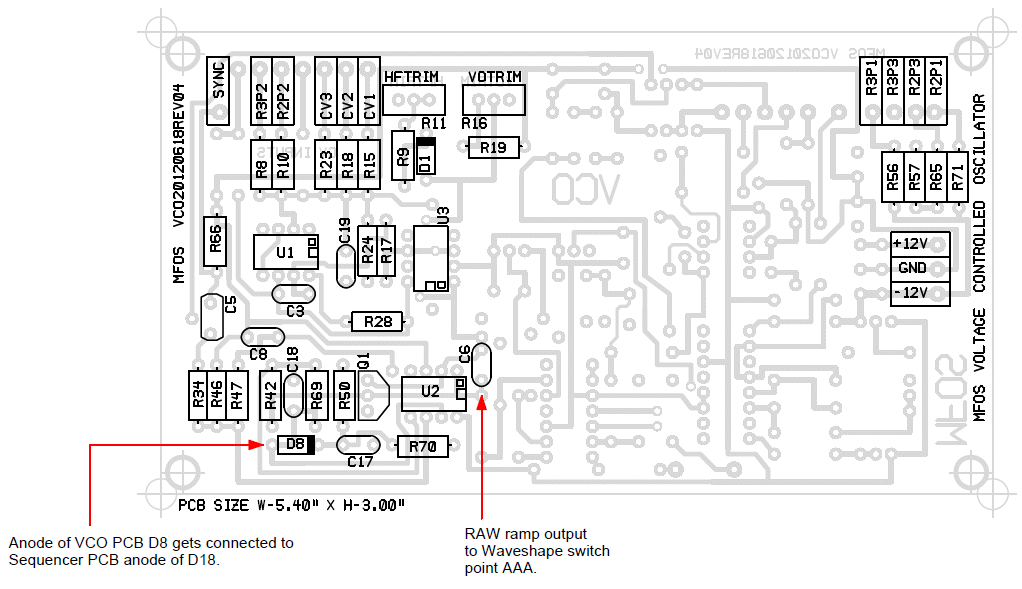
VCO PC Board Information
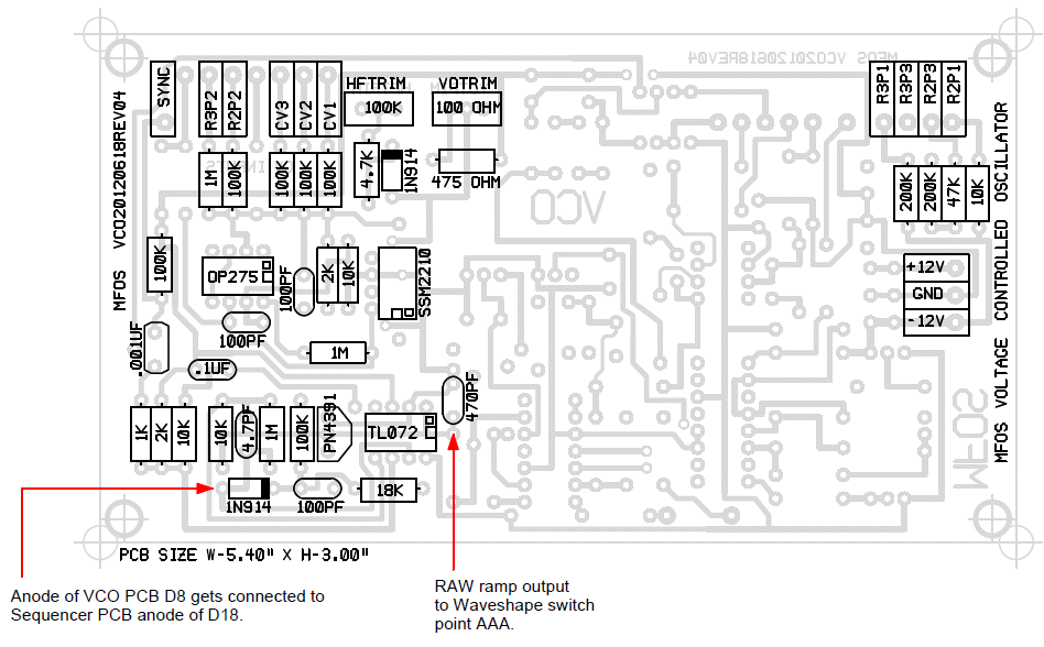
Parts Layout With Component Designators
Here we see where the clock signal from the VCO is connected to the Sequencer PCB. Wrap one end of the connecting wire around the anode lead of D8. The other end of the wire goes to the pad shown on the Sequencer PCB that connects to the anode of Sequencer PCB D18. See the sequencer PCB diagrams below.
The output of the ramp generator is wired to the Waveshape switch shown on the front panel wiring diagram (Point AAA).
Parts Layout With Component Values
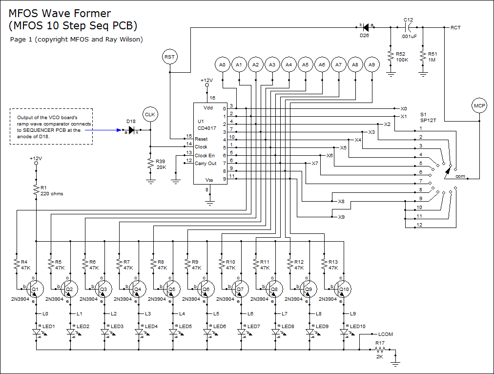
10 Step Sequencer Schematic (For use in Wave Former)
View as PDFFor this project much of the Sequencer circuitry has been eliminated. You can see where the VCO's comparator connects to the anode of D18 and then the positive excursions of the VCO comparator's output are fed to Sequencer circuit point CLK. This is the clock input of the CD4017B.
The common pole of the Wave Segments selector switch goes directly to the PCB point RCT. Thus the sequencer resets when it gets to the terminal count.
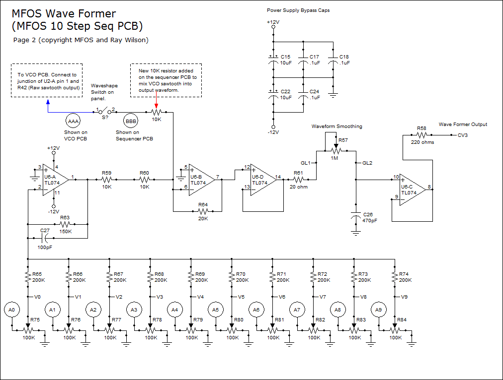
VCO Schematic
View as PDFThe main change for this part of the schematic is that a 10K resistor is added to the Sequencer PCB (shown on the sequencer PCB diagram). One end of the resistor connects to the inverting input of U6-B and the other end gets connected to one pole of the SPST Waveshape switch. When off the output of the Wave Former has square components and when on the output consists of sawtooth components. The original ramp fed into U6-B is inverted into a sawtooth shape. The other pole of the Waveshape switch connects to the RAW ramp output from the VCO (shown on the VCO PCB diagram).
The value of the Sequencer's glide capacitor C26 gets changes to 470pf and R57 adjusts the shape of the output by integrating it resulting in rounded corners of the square components. The range of filtering works well for the audio frequency output of the sequencer used in this manner.
10 Step Sequencer PC Board Information
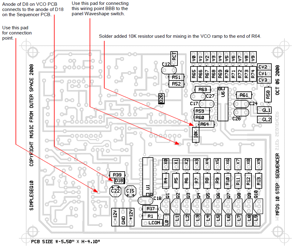
Parts Layout With Component Designators
Connections for the Waveshaper switch are shown here as well as the injection of the VCO's comparator output to be used for the sequencer's clock input.
Parts Layout With Component Values
Scope Shots
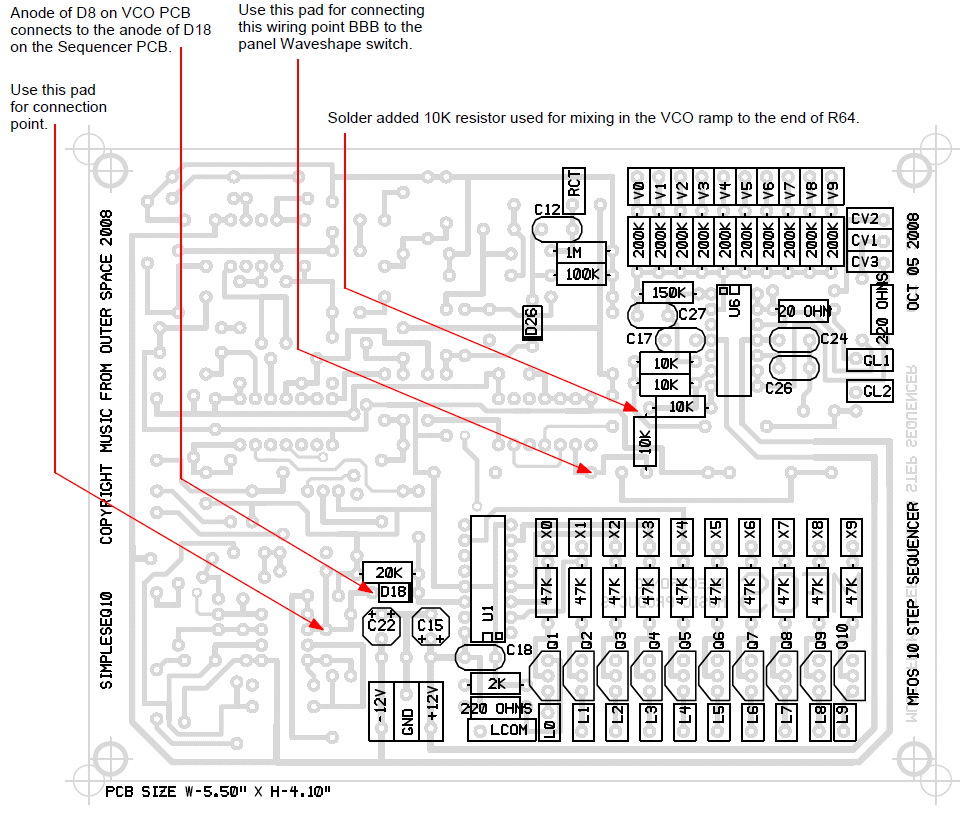
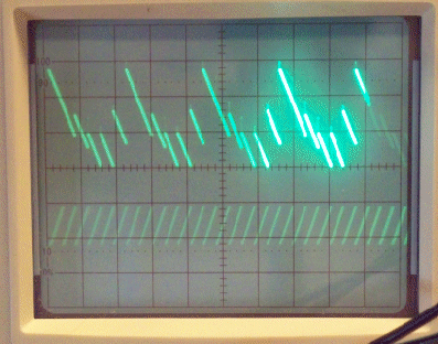
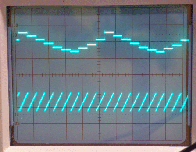
| Mixing the VCO's ramp wave into the output of the Sequencer's voltage results in waveforms like this. The sawtooth that rides on each of the levels can be moved up and down to create interesting waveforms and timbres. The bottom trace is the VCO's ramp wave. | Here we see a stepped sawtooth wave loaded with harmonics. The bottom trace is the VCO's ramp wave. | |
 |
 |
|
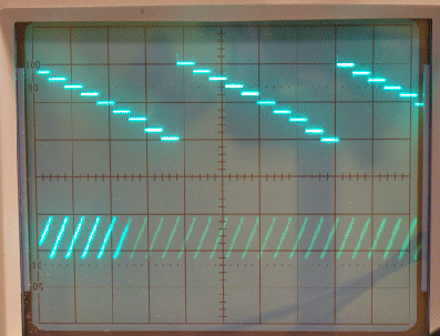
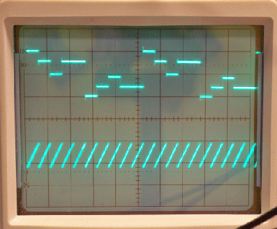
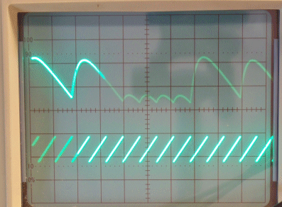
| This wave has a mix of square waves contributing harmonics to the total waveform. The bottom trace is the VCO's ramp wave. | Here we see a stepped triangle wave loaded with harmonics. The bottom trace is the VCO's ramp wave. | |
 |
 |
|
| Here we are using the sawtooth shape and applying adjustable low pass filtering using the glide of the sequencer to low pass filter the output of the sequencer. The bottom trace is the VCO's ramp wave. | ||
 |
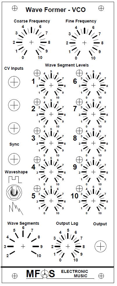
Wave Former Front Panel Information
Suggested Front Panel Layout
View as PDFCircuit Description
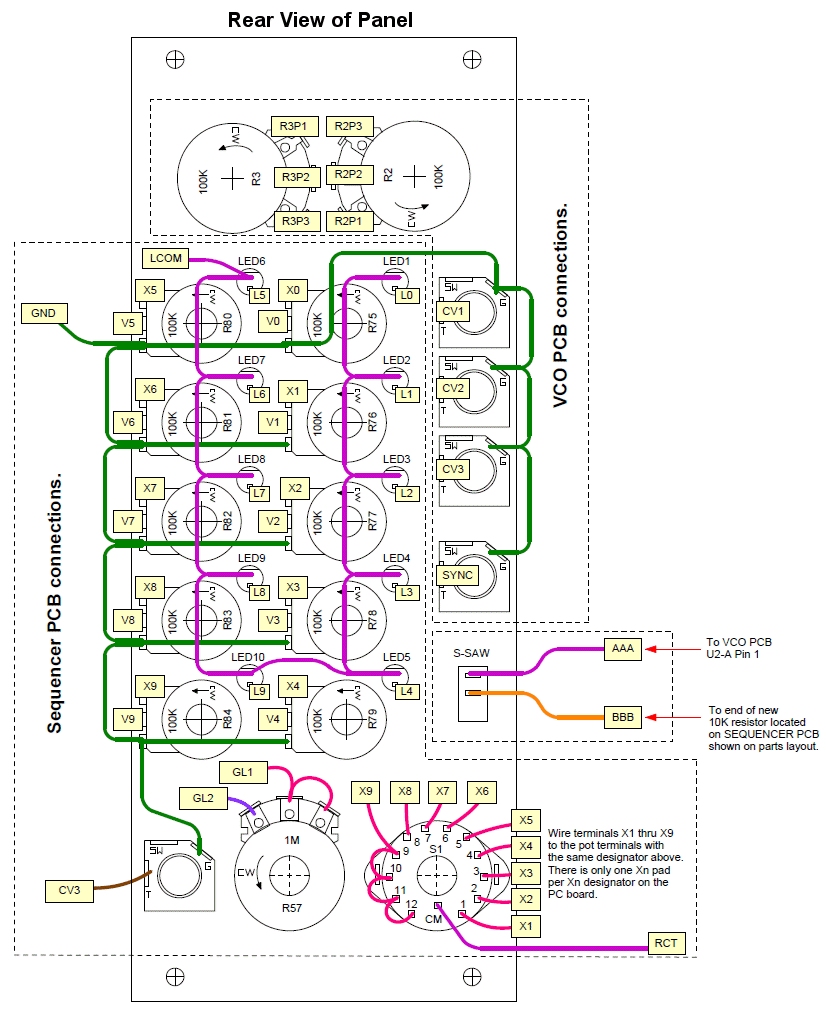
Suggested Front Panel Wiring Diagram
View as PDFCircuit Description
Echo Rockit Project Parts List
Component Notes
All cap voltages should be 25V or more. All resistors are 1/4W 5% (1% will work fine). MFOS PC boards use dual inline IC packages. MFOS PC boards usually use 5mm (0.2") cap lead spacing unless it is obvious from the board's legend that it should be larger or smaller. I often specify axial leads for any caps mounted on the front panel but you can use radial as well by adding some wire to the leads.
A SOIC package SSM2210 or SSM2212 can be used with the surface mount pads provided.
Use an op amp with good DC specs for U1. The OP275 is not mandatory.
VCO - Reduced Parts List for using PCB in Wave Former
| Qty. | Description | Value | Designators |
|---|---|---|---|
| 1 | OP275 Dual BiFET Op Amp | OP275 | U1 |
| 1 | SSM2210 Matched NPN Pair | SSM2210 | U3 |
| 1 | TL072 Dual Op Amp | TL072 | U2 |
| 1 | PN4391 N Channel JFET | PN4391 | Q1 |
| 2 | High Speed Switching Diode | 1N914 | D1, D8 |
| 2 | Linear Taper Potentiometer | 100K | R2, R3 |
| 6 | Metal Film 1/4 Watt 1% Resistor | 100K | R10, R15, R18, R23, R50, R66 |
| 4 | Metal Film 1/4 Watt 1% Resistor | 10K | R17, R42, R47, R71 |
| 1 | Metal Film 1/4 Watt 1% Resistor | 18K | R70 |
| 1 | Metal Film 1/4 Watt 1% Resistor | 1K | R34 |
| 3 | Metal Film 1/4 Watt 1% Resistor | 1M | R8, R28, R69 |
| 2 | Metal Film 1/4 Watt 1% Resistor | 200K | R56, R57 |
| 2 | Metal Film 1/4 Watt 1% Resistor | 2K | R24, R46 |
| 1 | Metal Film 1/4 Watt 1% Resistor | 4.7K | R9 |
| 1 | Metal Film 1/4 Watt 1% Resistor | 475 ohm | R19 |
| 1 | Metal Film 1/4 Watt 1% Resistor | 47K | R65 |
| 1 | Trim Pot 10 Turn | 100 ohm | R16 |
| 1 | Trim Pot 10 Turn | 100K | R11 |
| 1 | Ceramic Capacitor | .001uF | C5 |
| 1 | Ceramic Capacitor | .1uF | C8 |
| 3 | Ceramic Capacitor | 100pF | C3, C17, C19 |
| 1 | Ceramic Capacitor | 4.7pF | C18 |
| 1 | Silvered Mica Cap | 470pF | C6 |
10 Step Sequencer - Reduced Parts List for using PCB in Wave Former
| Qty. | Description | Value | Designators |
|---|---|---|---|
| 1 | +12 Volts | +12V | +12V |
| 1 | -12 Volts | -12V | -12V |
| 1 | CD4017 Decade Counter Decoder | CD4017 | U1 |
| 1 | TL074 Quad Op Amp | TL074 | U6 |
| 10 | 2N3904 | 2N3904 | Q1, Q2, Q3, Q4, Q5, Q6, Q7, Q8, Q9, Q10 |
| 2 | 1N914 Sw. Diode | 1N914 | D18, D26 |
| 10 | LED | LED | LED1, LED5, LED7, LED8, LED9, LED10, LED6, LED4, LED3, LED2 |
| 10 | Potentiometer | 100K | R75, R76, R77, R78, R79, R80, R81, R82, R83, R84 |
| 1 | Potentiometer | 1M | R57 |
| 3 | Resistor 1/4 Watt 1% | 10K | R59, R60, R64 |
| 1 | Resistor 1/4 Watt 1% | 150K | R63 |
| 1 | Resistor 1/4 Watt 1% | 20 ohm | R61 |
| 10 | Resistor 1/4 Watt 1% | 200K | R65, R66, R67, R68, R69, R70, R71, R72, R73, R74 |
| 1 | Resistor 1/4 Watt 1% | 20K | R64 |
| 2 | Resistor 1/4 Watt 1% | 220 ohms | R1, R58 |
| 1 | Resistor 1/4 Watt 1% | 2K | R17 |
| 10 | Resistor 1/4 Watt 1% | 47K | R4, R5, R6, R7, R8, R9, R10, R11, R12, R13 |
| 1 | Resistor 1/4 Watt 5% | 100K | R52 |
| 1 | Resistor 1/4 Watt 5% | 1M | R51 |
| 1 | Resistor 1/4 Watt 5% | 20K | R39 |
| 1 | Capacitor Ceramic | .001uF | C12 |
| 3 | Capacitor Ceramic | .1uF | C17, C18, C24 |
| 1 | Capacitor Ceramic | 100pF | C27 |
| 1 | Capacitor Ceramic | 470pF | C26 |
| 2 | Capacitor Electrolytic | 10uF | C15, C22 |
| 1 | 12 Pole Rotary Switch | SP12T | S1 |
| 1 | Switch SPST | SPST | S-SAW |
Project Notes
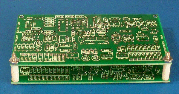
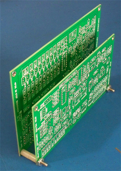
After population and wiring the VCO PCB can be mounted on the Sequencer PCB as shown. Although the holes are off by 0.1" a pair of 1 1/4" 6-32 machine screws can be used with standoffs and nuts to hold the two boards together as shown. The connected pair can then be mounted behind the panel.
Two PC Board Assembly