Article by Ray Wilson
Features
- State Variable VCF 12dB/Octave With VC Resonance
- Simultaneous High-Pass, Low-Pass and Band Pass Filter outputs.
- Log Response to Control Voltage (1V/Oct Tunable)
- Sine Wave Oscillator at full resonance
- Power Supply Range +/-9V up to +/-15V
- Voltage Controlled Resonance (Linear control)
Introduction
Voltage Controlled Filters are, in my opinion, one of the coolest modules in any synthesizer. They can subtract or add harmonics from the original signal and dynamically change the harmonic content as they are swept by external control voltages or track the keyboard voltage used to control your oscillators. I love the sound of a couple of oscillators tuned low and close to unison put through a low pass filter with a fair amount of resonance. As you modulate the cut off frequency (also in the low range) it has the sound of an airplane passing overhead or a hoomy singer modulating the frequency content of their droning chant by formant filtering with the mouth and throat. And of course white noise through a slowly modulated resonant filter sounds like you're out on the frozen tundra. This filter includes simultaneous high-pass, low-pass and band pass outputs, voltage controllable cut off frequency and resonance (or Q) giving your imagination even more variables to play with as you experiment with sounds. Additionally it provides inputs for a three-signal mixer. This filter puts me in mind of the words of the Jamaican car salesman I purchased my MPV van from many years ago but instead of "Mahn you gonna love daht vahn mahn" I say to you... Mahn you gonna love daht filter Mahn.
State Variable VCF 12dB/Octave With VC Resonance (All ADSR and LFO) MP3 SamplesInput was two low frequency square waves. Low Pass No Resonance Band Pass No Resonance Hi Pass No Resonance Low Pass Half Resonance Band Pass Half Resonance Hi Pass Half Resonance Low Pass Full Resonance (Oscillation) Band Pass Full Resonance (Oscillation) Hi Pass Full Resonance (Oscillation) |
|
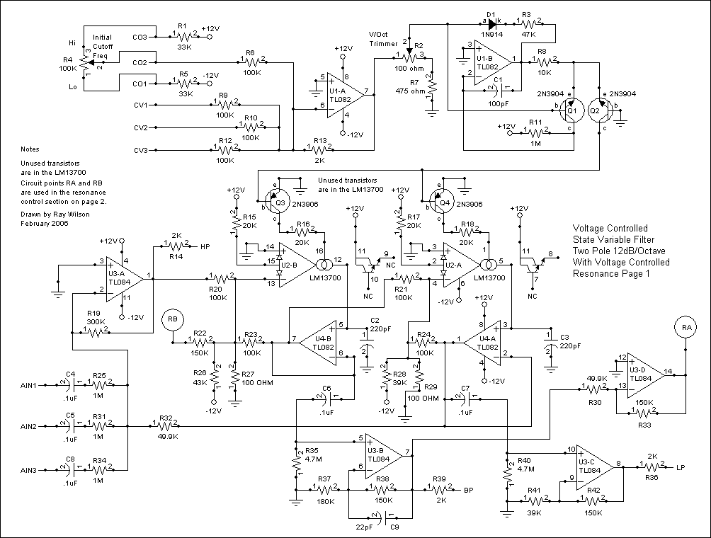
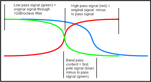
Up to 3 signal inputs can be applied to circuit points AIN1 thru AIN3. The .1uF input caps into 1 meg input resistors reduces the high pass effect that a smaller input resistor would have since pin 2 of U3-A is a virtual ground. Square waves of relatively low frequency will not differentiate too badly thus preserving their low frequency content. Signal levels of +/-5V are expected. If you have higher signal levels then reduce the value of R19 to insure that U3-A is not clipping when you feed in your signals. The opposite would be true as well (for lower levels increase the value of R19 to get adequate signal to noise ratio). U3-A acts as an active mixer with a gain of .30 (with values shown). The output of U3-A is fed into the filter via R20. The high pass output appears at the output of U3-A also and is fed to the HP output via R14 2K. The suggested panel layout shows jacks and three pots used as adjustable voltage dividers (level controls) to provide an input mixer for the unit. The jacks and mixer pots are not shown on the schematic. This VCF uses LM13700 transconductance amplifiers as voltage-controlled integrators. There are two of them in a chain and they operate in the same way. U2-B's transconductance is controlled by current flowing from ground via Q3 and R16 into U2-B pin 16. It acts like a voltage-controlled resistor that in conjunction with C2 is an RC filter. Since the output of U2-B is a current the signal is actually integrated onto C2. The filtered (actually integrated) signal is buffered by U4-B and fed to the next stage (a portion is also fed back to the input of U2-B via R23). R15 is used to bias the LM13700 linearizing diodes on (which is advertised to reduce distortion through the amp). R26 compensates for the positive offset applied via R15 (yes it goes to -12 but its applied to the inverting input). The goal is to keep the signal path of the system as close to operating about ground as possible. In practice you will see as high as +/-200 to +/-300 mV of offset at any of U4's outputs but that's fine. If things were operating near the rails we would have a problem. Here's my LAME-O explanation of how this works in laymans terms (the only terms I know). In order to obtain the state variable function notice that the low pass signal (at pin 1 of U4-A) is fed back to the inverting summer (U3-A and associated components) via R32 49.9K resistor. This in essence causes the low pass signal to be subtracted from the original signal resulting in high pass output at U3-A pin 1. The band pass output sounds like it consists of the difference between the output of the first filter pole and the low pass output. This drawing helps me to visualize this concept.
If this is so off base that it offends any math-savvy electronics genius types please feel free to submit your explanation. If you want a far more detailed and exact description of the theory of State Variable Filters check out Rayal Johnson's excellent paper Programmable State-Variable Filter Design For a Feedback Systems Web-Based Laboratory. Oh and go dig up your big-ass HP graphing calculator... cause you're gonna need it. Each filter section contributes 6dB/octave filtering (thus the two together result in 12dB/octave). The cut-off frequency control voltage inputs (CV1, CV2 and CV3) are applied to U1-A via the 100K input resistors R9, R10, and R12. Control voltage of between -5V and +10V are expected. Initial Cutoff Frequency control (R4) is used to set the initial cut-off frequency. R1 and R5 limit the range of voltage available at the wiper of R4 in the extreme positions. The summed control voltages are inverted by U1-A (inverting amp gain of .02) and fed to trimmer R2. The 20mV per volt output from U1-A can be trimmed to the requisite 18mV/volt by R2 that drives logging transistor Q1 to achieve a 1V/oct response in filter cut-off frequency. Current through Q1 is mirrored by Q2 that controls the current flowing from emitter to collector in Q3 and Q4. These transistors (Q3, Q4) control the current flowing from the "amp bias input" pins of the LM13700s to ground via current limiting resistors (R16 and R18). The result is that both integrators are controlled simultaneously. Since both are tuned to the same cut-off frequency very little signal above the cut-off frequency gets through the low pass portion. The low pass output is critical to the operation of the other filter modes (as described above). U3-C (and associated components) buffers and amplifies the low pass output. U3-B (and associated components) buffers and amplifies the band pass output. U3-A (and associated components) is the input mixer and doubles as the high pass output buffer. All filter outputs are protected against shorts by 2K resistors. The band pass output is is inverted and given a gain of 3 by U3-D which feeds the resonance/feedback circuit (Point RA). |
State Variable VCF 12dB/Octave With VC Resonance Schematic Page 2 PDF
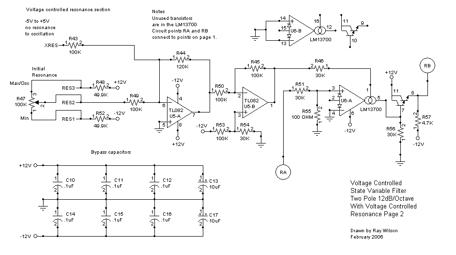
Point RA pg.1 (U3-D pin 14) connects to corresponding point RA pg.2 (R51 pin 1). R51 goes to the non-inverting input of U6-A (LM13700 transconductance amp) that controls the amount of negative feedback applied to the input of the filter (point RB pg.2 connects to corresponding point RB pg.1). Adding negative feedback results in the characteristic filter ringing that adds interesting harmonics to the original signal. You will also notice that the output signal level will decrease as the feedback is increased. Simultaneously the amplitude of the ringing will increase. This control is referred to as resonance because the harmonic content of the original signal is accentuated when the control is advanced. At maximum feedback the circuit will produce a very pure sine wave that can be used as a pitch source or control voltage. When the resonance is at about mid level and noise is used as the input signal the output will produce pitched noise. The resonance control circuit simply applies from ground to -10 volts to R46 that controls the "amp bias input" of U6-A and thus its transconductance linearly. The resonance control signal XRES is expected to be -5V to +5 volts.
| Approx. Current Consumption | |
| +12V | 30mA |
| -12V | 30mA |
| +15V | 32mA |
| -15V | 32mA |
You can use just about any general purpose BIFET opamp for the TL084 (quad) and TL082 (dual) and you can sub any of these (LM13600, NE5517, AU5517, NTE870) for the LM13700. General purpose NPNs can be used for Q1 and Q2 and their PNP counterparts should be used for the PNPs. Rev 002 boards accept 8 pin DIP packages for transistor pair packages.
As usual I must disclaim any credit regarding the invention of these concepts. The Don Sauers, Robert Moogs and Bernie Hutchins of the world figured all of these concepts out. I am merely implementing my version of it. Acknowledgements Page
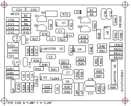
State Variable VCF 12dB/Octave With VC Resonance PCB Parts Layout (Parts Side Shown) PDF
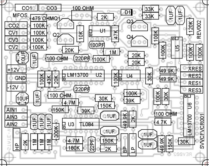
State Variable VCF 12dB/Octave With VC Resonance Component Value View
State Variable VCF 12dB/Octave With VC Resonance PCB Bottom Copper (Parts Side Shown)
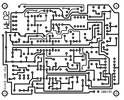
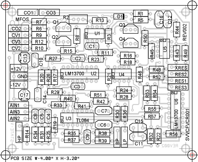
State Variable VCF 12dB/Octave With VC Resonance PCB Top Copper(Parts Side Shown)

State Variable VCF 12dB/Octave With VC Resonance PCB Top Silk Screen
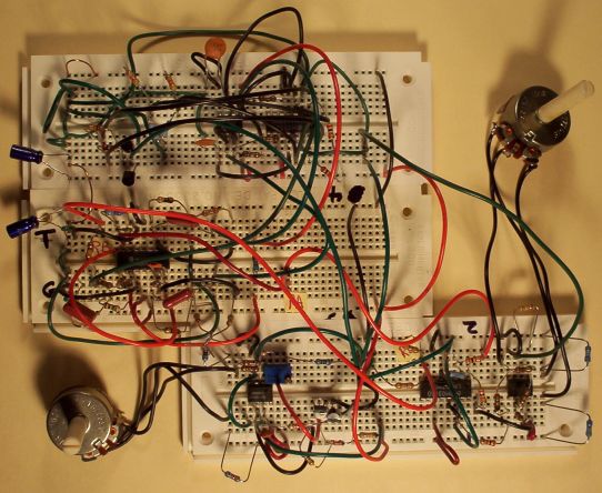
State Variable VCF 12dB/Octave With VC Resonance on the Breadboard
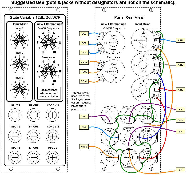
State Variable VCF 12dB/Octave With VC Resonance Front Panel and Wiring PDF
The jacks and mixer pots shown in this suggested layout are not on the schematic. Use whatever jacks you are using in your system. The suggested mixer pots are 100K linear taper (log taper would also work fine). This suggestion is provided merely as an example or wiring guide.
State Variable VCF 12dB/Octave With VC Resonance Project Parts List
I specify all resistors as 1% but 5% will work. Metal film 1% will give you better temperature stability. Capacitors can be film, ceramic, or silver mica. The 220pF integrator caps should be high quality and well matched for best results. You can use just about any general purpose BIFET opamp for the TL084 (quad) and TL082 (dual) and you can sub any of these (LM13600, NE5517, AU5517, NTE870) for the LM13700.MFOS State Variable Filter Project Parts List
| Qty. | Description | Value | Designators |
|---|---|---|---|
| 2 | LM13700 Dual gm OpAmp(s) | LM13700 | U2, U6 |
| 3 | TL082 Dual Op Amp(s) | TL082 | U1, U4, U5 |
| 1 | TL084 Quad Op Amp | TL084 | U3 |
| 1 | 1N914 Sw. Diode | 1N914 | D1 |
| 2 | 2N3904(s) | 2N3904 | Q1, Q2 |
| 2 | 2N3906(s) | 2N3906 | Q3, Q4 |
| 11 | Ceramic Capacitor (S)(s) | .1uF | C6, C7, C4, C5, C8, C11, C15, C16, C12, C10, C14 |
| 1 | Ceramic Capacitor (S) | 100pF | C1 |
| 2 | Ceramic Capacitor (S)(s) | 220pF | C2, C3 |
| 1 | Ceramic Capacitor (S) | 22pF | C9 |
| 2 | Electrolytic Capacitor (S)(s) | 10uF | C13, C17 |
| 2 | Potentiometer(s) | 100K | R4, R47 |
| 1 | Trim Pot | 100 ohm | R2 |
| 2 | Resistor 1/4 Watt 1%(s) | 49.9K | R52, R48 |
| 3 | Resistor 1/4 Watt 5%(s) | 100 OHM | R27, R29, R55 |
| 13 | Resistor 1/4 Watt 5%(s) | 100K | R21, R9, R12, R10, R6, R24, R20, R23, R49, R45, R53, R50, R43 |
| 1 | Resistor 1/4 Watt 5% | 10K | R8 |
| 1 | Resistor 1/4 Watt 5% | 120K | R44 |
| 4 | Resistor 1/4 Watt 5%(s) | 150K | R38, R42, R22, R33 |
| 1 | Resistor 1/4 Watt 5% | 180K | R37 |
| 4 | Resistor 1/4 Watt 5%(s) | 1M | R11, R25, R31, R34 |
| 4 | Resistor 1/4 Watt 5%(s) | 20K | R15, R17, R16, R18 |
| 4 | Resistor 1/4 Watt 5%(s) | 2K | R13, R39, R36, R14 |
| 1 | Resistor 1/4 Watt 5% | 300K | R19 |
| 4 | Resistor 1/4 Watt 5%(s) | 30K | R56, R46, R54, R51 |
| 2 | Resistor 1/4 Watt 5%(s) | 33K | R1, R5 |
| 2 | Resistor 1/4 Watt 5%(s) | 39K | R41, R28 |
| 1 | Resistor 1/4 Watt 5% | 4.7K | R57 |
| 2 | Resistor 1/4 Watt 5%(s) | 4.7M | R35, R40 |
| 1 | Resistor 1/4 Watt 5% | 43K | R26 |
| 1 | Resistor 1/4 Watt 5% | 475 ohm | R7 |
| 1 | Resistor 1/4 Watt 5% | 47K | R3 |
| 2 | Resistor 1/4 Watt 5%(s) | 49.9K | R32, R30 |
Miscellaneous
- (1) 1/16" Thick aluminum plate for mounting the pots and switches.
- Unit is typically mounted in a synth case with other synth modules.
- Assorted hardware 1" 6-32 nuts and bolts, 1/2" #8 wood screws, etc
- Knobs for potentiometers, wire, solder and typical assorted electronics hand tools.
- Digital Volt Meter and a Signal Tracer or oscilloscope for testing.