Ray Wilson authored this content while he was actively running MFOS as the founder and resident genius.
We retain the content because it reflects a valuable point of view representing that time and place.
Article by Ray Wilson
Table of contents
- Schematic Page 1 Sound Lab Mini-Synth Mark II 12dB/Octave State Variable VCF
- Schematic Page 2 Sound Lab Mini-Synth Mark II VCO1 and VCO2
- Schematic Page 4 Sound Lab Mini-Synth Mark II White Noise Generator
- Schematic Page 5 Sound Lab Mini-Synth Mark II Audio Mixer
- Schematic Page 6 Sound Lab Mini-Synth Mark II AD Envelope Generators
- Schematic Page 7 Sound Lab Mini-Synth Mark II Low Frequency Oscillator
- Schematic Page 8 Sound Lab Mini-Synth Mark II Voltage Controlled Amplifier
- Schematic Page 9 Sound Lab Mini-Synth Mark II Sample & Hold
- Sound Lab Mini-Synth Mark II Calibration
The Sound Lab Mini-Synth Mark II consumes approximately 75 to 80 mA from the +12V rail and about 75 to 80 mA from the -12V rail. I recommend using the same supply voltages I did (+/-12V). If you decide to go to +/-15V you may need to change bias where resistors are used to create a voltage level. I do not plan to evaluate the unit on +/-15V and again recommend +/-12V. An MFOS wall wart supply will be more than adequate to power this synth.
Schematic Page 1 Sound Lab Mini-Synth Mark II 12dB/Octave State Variable VCF
View as PDF
The 12db/octave state variable filter works as follows. Control voltages are applied to the control voltage summer U1-A via the 100K resistors feeding it's inverting input. The fine COF pot feeds the control voltage summer via a 4.7M resistor (R35) so that the fine pot gives a much smaller range of adjustment to the cut off frequency. The filter goes from sub audible to about 18kHZ at the top end. The VCF modulation sources: LFO and AD1 (Attack Decay Envelope Generator 1) are fed into the control voltage summer via linear 100K pots R9 and R13 (wired as variable voltage dividers) respectively to allow for adjustment of the modulation levels of those sources. Switch S20 lets you add keyboard voltage as a modulation source for the VCF. The output of the control voltage summer feeds the voltage to exponential current convertor (U1-B and associated components). It is important to use a matched pair of NPN transistors for Q1 and Q2. The critical parameter for the transistors is that their VBE be within 2mV of one another. I also recommend that Q3 and Q4 be a matched pair of PNP transistors with VBE within 2mV of one another. I sell matched pairs both discrete and the SSM2210 integrated matched pair. Here is some information on matching transistors. The expo convertor's whole job in life is to convert the voltage presented to it via the control voltage mixer into current. But the conversion factor is very critical if you want the VCF to track 1V/octave. The transistor in the feedback loop of U1-B (Q1 2N3904) is the magic component. It doubles it's current output for every approximate 18mV change in voltage presented to it's base. So the 100 ohm trimmer R12's job is to adjust the voltage fed to the base of Q1 so that you apply the exact voltage change necessary to get the current doubling response. Current through Q1 is mirrored in Q2 and Q2's current is applied to the bases of Q3 and Q4 who also mirror (but invert) the current flowing into the LM13700 bias inputs from ground. The potential at the bias inputs is low so current can flow from ground into the bias inputs. The 10K resistors Q3 and Q4 act to keep the current into the bias inputs limited and balanced. The high frequency compensation adjustment trimmer is necessary because without it the filter's cutoff frequency would go flat at higher frequencies due to the bulk emitter resistance of transistor Q2. (For an excellent article on Log and Exponential (Antilog) Circuits see Bernie Hutchins' ELECTRONOTES S-019).

The LM13700 transconductance op amps act like current controlled resistors and change in proportion to the current flowing into their bias pins. Thus the cut off frequency of the filter increases as more voltage is applied to the control voltage mixer's input(s). The cut off frequency goes lower as lower voltage is applied to the control voltage mixer's input(s). The LM13700 state variable filter is based on the example presented in the National Semiconductor datasheet for the LM13700. I added the N Channel JFET buffers to increase the impedance of the amplification stage buffering the integrating capacitors. Doing so allows the filter to produce clean sine oscillation when in low pass mode and the resonance control is turned so that there is a lot of positive feedback around U2-A (resonance control is turned up). Two of the state variable filter's outputs are used: low-pass and band-pass. In band pass mode I find I need to reduce the mixer input levels to avoid distortion. To avoid adding non-linear distortion to the signal fed to the input of the VCF via C2 it has to be significantly attenuated which is the job of the resistor divider formed by R24 (100K resistor) and R25 (1K resistor). Also note that the output of the first filter section is applied to the second section via another resistive attenuator R21 (100K resistor) and R23 (220 ohm resistor). Switch S1 lets you select which of the filter's outputs is connected to the VCA's input.
VCF Sanity Check Measurements
You should see something reasonably close to what I am showing here when you measure the points specified below.
| Coarse Pot Setting | Fine Pot Setting | Circuit Point Measured | Approximate Value |
|---|---|---|---|
| Fully off | N/A | Coarse COF Adjust R1 100K Pot's Wiper | -5V |
| Fully on | N/A | Coarse COF Adjust R1 100K Pot's Wiper | +8.5V |
| N/A | Fully off | Fine COF Adjust R34 100K Pot's Wiper | -12V |
| N/A | Fully on | Fine COF Adjust R34 100K Pot's Wiper | +12V |
| Fully off | Fully off | U1-A Pin 1 | 110 mV |
| Fully on | Fully off | U1-A Pin 1 | -165 mV |
| Fully off | Fully on | U1-A Pin 1 | 100 mV |
| Fully on | Fully on | U1-A Pin 1 | -175 mV |
| Fully off | Fully off | U1-B Pin 7 | -55 mV |
| Fully on | Fully off | U1-B Pin 7 | -4.1 V |
| Fully off | Fully on | U1-B Pin 7 | -56 mV |
| Fully on | Fully on | U1-B Pin 7 | -4.85 V |
| Fully off | Fully off | U2-A Pin 1 | -11 V |
| Fully on | Fully off | U2-A Pin 1 | -10.75 V |
| Fully off | Fully on | U2-A Pin 1 | -10.75 V |
| Fully on | Fully on | U2-A Pin 1 | -10.73 V |
| Fully off | Fully off | U2-A Pin 5 | -386 mV |
| Fully on | Fully off | U2-A Pin 5 | -1.65 V |
| Fully off | Fully on | U2-A Pin 5 | -600 mV |
| Fully on | Fully on | U2-A Pin 5 | -1.63 V |
| Fully off | Fully off | U2-B Pin 12 | -45 mV |
| Fully on | Fully off | U2-B Pin 12 | -2.44 V |
| Fully off | Fully on | U2-B Pin 12 | -62 mV |
| Fully on | Fully on | U2-B Pin 12 | -2.46 V |
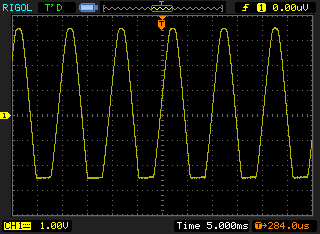
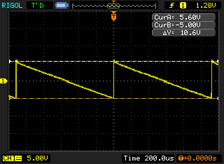
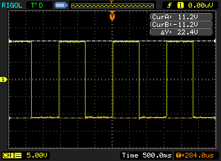
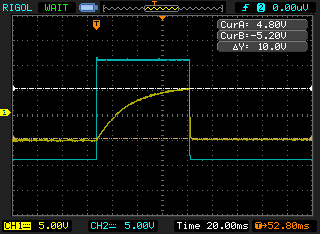
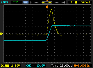
VCF Scope Photos
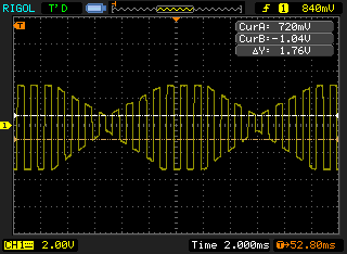
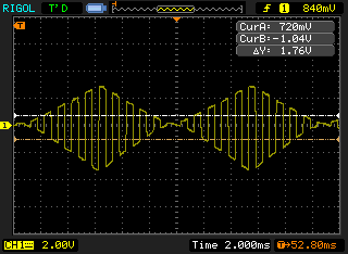
Settings are shown in the first cell and then only the changes are shown. The last image illustrates that when using the filter as a sine wave osccillator you need to select the "Low Pass" response. When "Band Pass" response is selected there will be a distortion in the sine waveform. When filtering with high resonance in band pass mode I suggest that you reduce the signal levels via the mixer to avoid clipping or distortion (unless you like it :-)).These are scope photos of the main output of the unit.
|
|
|
|
|
|
|
|
|


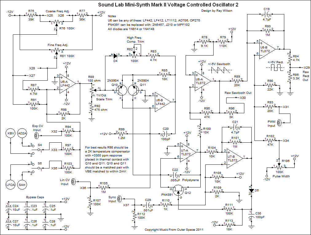
Schematic Page 2 Sound Lab Mini-Synth Mark II VCO1
View as PDFThe Sound Lab Mini-Synth Mark II has two identical VCOs. I will describe the operation of VCO1. VCO2 operates in an identical manner.
Again we see a control voltage summer followed by a voltage to exponential current convertor that looks very similar to the one used for the VCF. In this case we do not invert the sense of the current from the expo current generator. Instead the current that flows into the collector of Q8 is used to cause the integrator which functions as the heart of the oscillator to ramp up at a rate which is directly porportional to the amount of current flowing into the collector of Q8. Again we have the high frequency compensation circuit that helps to mitigate high end oscillator flatness. In this case two factors are compensated for at once. Both the bulk emitter resistance issue of Q8 and the ramp core reset time. (For an excellent article on Log and Exponential (Antilog) Circuits see Bernie Hutchins' ELECTRONOTES S-019) Both of those factors tend to cause the oscillator to become flat at high frequencies (high in this case being above about 2KHz). After the synthesizer if completed you must calibrate the VCO scale factor (using trimmer R49) and high frequency compensation (using trimmer R43). Again it is very important to use a well matched pair of discrete NPN transistors (2N3904, 2N2222, etc) or a chip containing matched NPN transistors (SSM2210 for example). For temperature compensation R59 should be a 2K +3300 ppm temperature compensator. To get things working you can use an unmatched pair of NPN transistors for Q7 and Q8 and a regular 2K resistor for R59. I sell both matched discrete NPN (and PNP) transistors and 2K 2% 1/4 watt +3300 ppm temperature compensators if you need them.
The oscillator has normallized switching for 1) keyboard voltage or Attack Decay Envelope Generator 1 (S2) and 2) LFO or Sample and Hold output (S3). Note that these switches are "center off" also specified as ON-OFF-ON by switch manufacturers and suppliers. The coarse frequency adjust and the fine frequency adjust pots (R37 and R42 100K linear pots) are used to set the starting frequency. Sources of control voltage and/or modulation then add or subtract from this frequency as they are applied resulting in frequency modulation.
NOTE! Circuit point X19 is on the PC board but there is no connection for it on the panel I sell. If you would like, you can add another VCO expo modulation input for VCO 1 by mounting an additional banana jack and connecting it to point X19.

The linear CV input (X23) changes the initial current setpoint of the expo convertor in a linear way. Modulation applied via this input will cause the oscillator to be modulated at far lower levels than applying modulation to the exponential CV inputs.
The only difference between VCO1 and VCO2 is that VCO2 has a banana jack input for sync and can be synced by the LFO for interesting sonic effects via patch cords. The sync input accepts a hard negative going step voltage to cause the VCO's integrator to reset. On reset the ramp core goes back to 0 volts and starts ramping up in response to the negative sync edge. The sync source oscillator's frequency is usually tuned lower than the oscillator being synced for interesting effects. In this case tuning VCO2 lower than VCO1 and then sweeping VCO1's frequency upward demonstrates the interesting timbres provided via sync. The negative step applied to the Sync input propogates through C17 (.001uF cap) and R71 (1K resistor) and pulls the reference set by R69 (10K resistor) and R70 (2K resistor) below the value on the non-inverting input (the ramp wave at the output of U4-A. This causes comparator U4-B to go high turning on Q9 (essentially shorting D to S) and resetting the integrator.
I specify LF442 in the schematic for the control voltage summer and expo convertor but the better the op amp used here (linearity, low input current, low offset) the better the tracking of the oscillator will be. I recommend OP275, LT1013, TL072 etc.
The VCO tracks up to about 4kHz with careful trimming but can go far higher in frequency. The VCO's range is from about 24 Hz to 20 KHz. I'm fine with this range but you can achieve lower range by adjusting the value of R36 down a bit (33K 30K etc) for VCO 1 and R75 down a bit (33K 30K etc) for VCO 2 if you desire it.
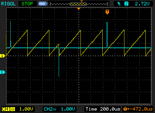
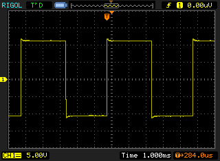
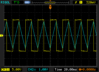
VCO Scope Photos
Settings are shown in the first cell and then only the changes are shown.
|
|

The output of the ramp core (pin 7 of U4-A) is fed to U5-A which acts as an inverting level shifter with gain of about -4.7. R39 and R40 bias the op amp so that the amplified signal oscillates about ground and has an amplitude of about +/-5V peak to peak. The output of U5-A becomes the sawtooth output (X17) of the oscillator via current limiting resistor R57. The output of U5-A is also fed via R50 (20K resistor) to the input of op amp U5-B which is used as a comparator. The output of U5-B goes high when the level on it's non-inverting input goes above the threshold held on the inverting input set by both the Pulse Width adjust pot and the external PWM voltage input. Adjusting R67 will vary the pulse width from approximately 10% to approximately 90%. If you desire more adjustment you can decrease the value of R63 somewhat so that the threshold levels on pin 6 set via R67 (100K Pulse Width pot) of U5-B can be increased. C7 (4.7pF capacitor) provides a burst of positive feedback which sharpens the corners of the rectangular wave at the output of U5-B. R41 (1M resistor) provides a bit of hysteresis so that the output of the rectangle wave does not chatter (rapidly oscillate high and low) as the sawtooth wave passes through the threshold on it's low to high or high to low transistions. The output of U5-A is attenuated to match the levels of the sawtooth wave by the resistive divider formed by R45 (4.7K resistor) and R47 (3.3K resistor). You can feed in a voltage to set the threshold level (via banana jack PWM). This can be the output of the LFO or an AD generator (or what have you...). When you slowly modulate the width of a rectangular wave (via connecting the LFO triangle wave to PWM) it sounds like two slightly de-tuned square waves beating against each other.
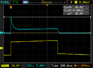
VCO Sanity Check Measurements
You should see something reasonably close to what I am showing here when you measure the points specified below.
| Coarse Pot Setting | Fine Pot Setting | Circuit Point Measured | Approximate Value |
|---|---|---|---|
| Fully off | N/A | Coarse Freq Adjust R37 100K Pot's Wiper | -5V |
| Fully on | N/A | Coarse Freq Adjust R37 100K Pot's Wiper | +5.4V |
| N/A | Fully off | Fine Freq Adjust R42 100K Pot's Wiper | -12V |
| N/A | Fully on | Fine Freq Adjust R42 100K Pot's Wiper | +12V |
| Fully off | Fully off | U3-A Pin 1 | 100 mV |
| Fully on | Fully off | U3-A Pin 1 | -100 mV |
| Fully off | Fully on | U3-A Pin 1 | 92 mV |
| Fully on | Fully on | U3-A Pin 1 | -115 mV |
| Fully off | Fully off | U3-B Pin 7 | -55 mV |
| Fully on | Fully off | U3-B Pin 7 | -5.00 V |
| Fully off | Fully on | U3-B Pin 7 | -55 mV |
| Fully on | Fully on | U3-B Pin 7 | -7 V |
| N/A | N/A | U4-B Pin 2 | 2 V |
| N/A | N/A | U5-B Pin 6 PW (R67) Set to 1/2 | 0 V |
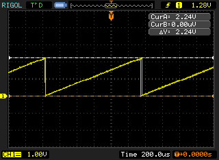
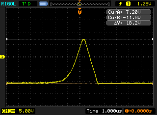
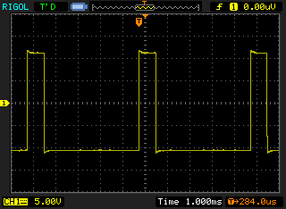
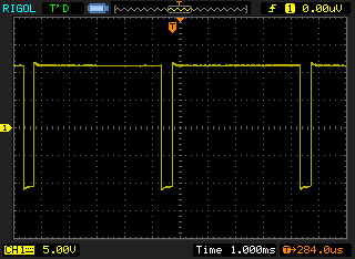
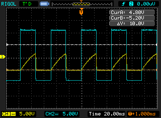
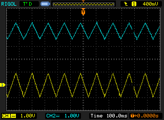
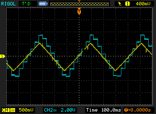
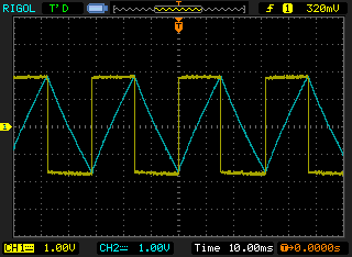
VCO1 Scope Photos
Settings are shown in the first cell and then only the changes are shown.
|
|
|
|
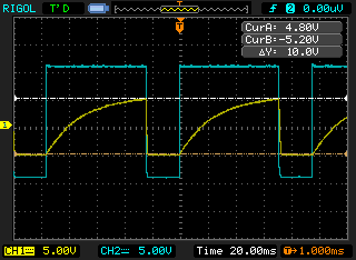
Rectangle Wave Output The rectangle/pulse wave output at the VCO outputs (U5-B pin 7 and U8-B pin 7) are opposite of what the front panel duty cycle legend says, however, the front panel legend is correct when the inversion that takes place in the synth's mixer is factored in. This is the synth output with one rectangle wave's volume turned up, cut off frequency turned fully up, resonance turned fully down, and no VCA modulation as the pulse width knob is adjusted.
|
||
|
|
|
Schematic Page 3 Sound Lab Mini-Synth Mark II VCO2
View as PDFAs explained above VCO2 operates in the same manner as VCO1. The only differences are that 1) VCO2 has normalized switching that allows choosing either keyboard voltage or Attack Decay Envelope Generator 2 (VCO1 permits selection between keyboard voltage or AD EG 1) and the sync input is a banana jack instead of a switched connection to the other VCO.
NOTE! Circuit point X32 is on the PC board but there is no connection for it on the panel I sell. If you would like, you can add another VCO expo modulation input for VCO 2 by mounting an additional banana jack and connecting it to point X32.
Schematic Page 4 Sound Lab Mini-Synth Mark II White Noise Generator
View as PDFThe white noise generator is very simple and uses the technique of exceeding the emitter to base breakdown voltage of an NPN transitor to produce white noise. Q13's emitter is connected to +12V via series connected 470K resistors R115 and R116 and its base is connected to ground. Thus the emitter to base breakdown voltage of about 5 or 6 volts is exceeded. Resistors R155 and R116 provide current limiting to prevent any damage to the reverse biased NP junction. Remove the noise transistor's collector since it is not connected and due to the high gain of the circuit it will act like an antenna possibly picking up 60 Hz. hum if you leave it attached. C31 is present to filter the voltage fed to the transistor's emitter. Typically you need to apply a lot of gain to bring the noise up to a usable level so we want to filter any noise (60 hz or otherwise) out of the voltage feeding the noise generator. The actual noise is generated at the junction of R116 and the Q13's emitter. We capacitivley couple the low level noise signal to the first amplifier stage (U9-A and associated components) where a gain of about 100 is applied. If you happen to have a really noisey transistor for Q13 that causes U9-B's output to clip or results in too high a level of noise on the output U9-B you can reduce the gain of the first stage by changing R121 to 2K or 3K if necessary to bring the level withing the recommended amplitude of +/-5V peak to peak. The output of U9-A is capacitively coupled to the second gain stage (U9-B and associated components) where an adjustable gain of between about 1 and 100 is applied. Adjust trimmer R123 so that there is a noise signal of about +/-5V peak to peak oscillating about ground. That means you want an average of 5V above ground and 5V below ground. The white noise is output via C34 and is applied to the mixer's White Noise pot and the front panel noise jack. You MUST select a good noise transistor from among several transistors in order to find one with sufficient noise. You should see at least 500mV to 1V p-p of noise from the first gain stage (U9-A pin 1). If you don't keep testing or... buy a pack of selected noise transistors with guaranteed 3V of noise from a non-inverting gain of 100 from me.
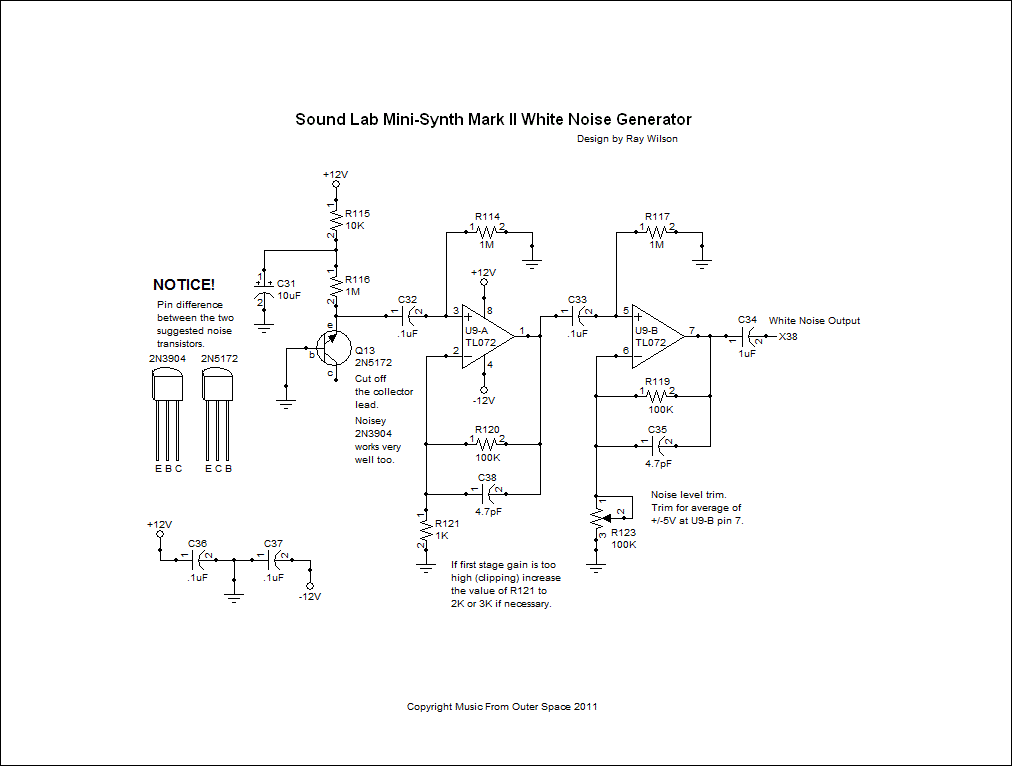
Here is what my noise output looks like on both the first stage and second stage of gain. Since the second stage gain can go to about 101 as long as the first stage is giving you at least 100 to 200 mV peak to peak you should be fine. Here we see that my first stage is outputting about 1.8V peak to peak which is good because the lower the required overall gain in this circuit the less 60 cycle or reflected signal noise gets into the white noise signal. A good noisey transistor is the linch-pin of this circuit (I finally got to use linch-pin in a sentence). If you like you can purchase pre-selected 2N5172 noise transistors from me.
White Noise Generator Scope Photos
|
|


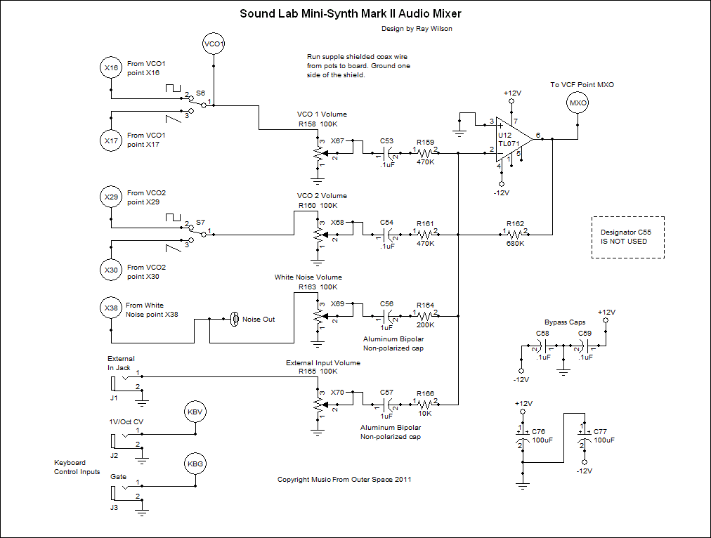
Schematic Page 5 Sound Lab Mini-Synth Mark II Audio Mixer
View as PDFThis is the audio mixer for the synth. It is a very simple design and uses an op amp as an inverting summer. VCO1 and VCO2 are both fed into the mixer via input level controls R158 (audio taper 100K pot) and R160 (audio taper 100K pot). The wipers on the pots are tied to .1uF caps in series with 470K resistors and to the inverting input of U12. The oscillator inputs can overdrive the mixer (and subsequently the VCF and VCA) when set to high levels.
The white noise is fed into the mixer via level set pot R163 (audio taper 100K pot) 1uF cap C56 and resistor R164 (200K). The noise can also overdrive the mixer op amp when set to high levels. I find I like to really pump the white noise for certain sounds and you have plenty of gain to play with. The raw noise signal is patched to the banana jack on the front panel so you can use it as an input to the sample and hold module.
The external input is connected to the op amp summer via R165 (100K pot), 1uF cap C57 in series with 10K resistor R166. The external input provides the most gain and can be used with line or instrument level signals. You really don't need to crank the external pot up much to get good guitar or keyboard levels to put through the synth's VCF and VCA.
Notice that the caps for both the noise and the external input are 1uF non-polarized caps to preserve the low frequency content of the signals (since the input resistors are quite a bit lower in value than for the VCOs). Since VCO1 and VCO2 both have 470K resistors in series with their DC blocking caps (C53 and C54 respectively) I used a lower value for them (.1uF). If you desire to, you can use higher values here (.22uF or .47uF) to get even less differentiation of the low frequency square and sawtooth waveforms but I'm very satisfied with the sound provided by the current values. The output of the mixer point (MXO) is connected to the input of the VCF.
The keyboard control jacks are shown on this page. The points KBV and KBG connect to the appropriate points on the panel for the normalized switching for the keyboard control connections of the VCOs and AD generators. You connect the control voltage output of your keyboard or sequencer to the jack marked "1V/Oct CV" and the gate output of your keyboard or sequencer to the jack marked "Gate". You need to turn the normalized switches to KBD CV or KBD Gate to control the synth's modules with the signals applied to these jacks.
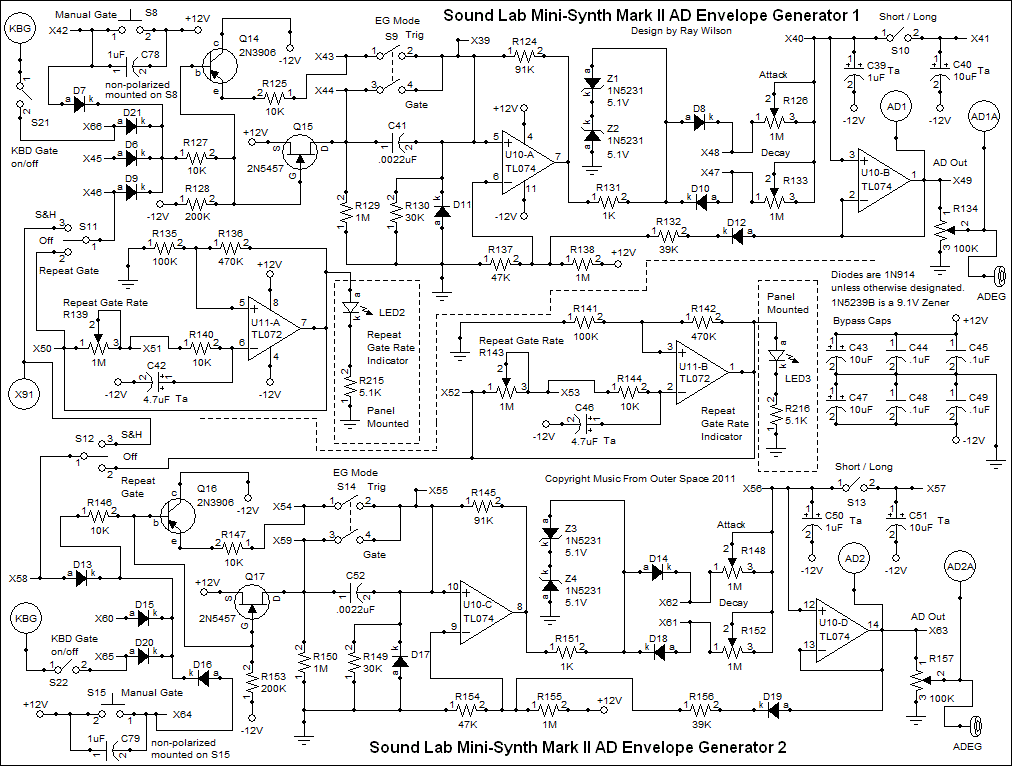
Schematic Page 6 Sound Lab Mini-Synth Mark II AD Envelope Generators
View as PDFThere are two identical AD Generators in the synth. One of them is dedicated to the VCF and one to the VCA. The outputs of the two are also available via front panel banana jacks for use in controlling VCO pulse width or as input to the Sample and Hold module. The normalized switching of the VCOs routes the outputs of the AD generators to the CV inputs of the VCOs for cool modulation effects. The level controls of the AD generators adjust the level of the envelope fed to the VCOs when they are connected for modulation via there KBD CV/ADx switches and the level of the signal fed to the respective ADEG Out banana jacks. Each of the AD generators has an associated Repeat Gate Generator the operation of which will also be described here. Only the operation of AD Envelope Generator 1 and it's associated Repeat Gate Generator will be described. AD Envelope Generator 2 works in an identical fashion (only the designators have been changed to protect the innocent).
Gate or trigger signals are routed to AD Generator 1 via connection to the anodes of 1N914 diodes D7, D21, D6 and D9. The gate must go from ground or below (the diodes block negative voltage anyway) to at least 3.5 or 4 volts DC. If any of these inputs is held high the AD generator will ignore the other inputs until the high level is removed.
Manual gate pushbutton S8 is used to apply a gate to the AD generator manually. The capacitor (C78 1uF non-polarized AL) which gets mounted across the terminals of pushbutton S8 minimizes gate switch bounce. The KDG Gate switch S21 is used to apply the gate signal connected to the unit's Keyboard Control Gate input when desired.
The gate signal applied to any of the input diode anodes pushes current through R127 (10K resistor) and drops voltage on R128 (200K resistor) whose other end is connected to -12V. The junction of R127 and R128 is connected to both the base of Q14 (2N3906 PNP transistor) and the gate of Q15 (2N5457 N channel JFET). Under "no gate or gate low" condition Q14 is turned on and Q15 is turned off. When a gate is applied the voltage at the junction of R127 and R128 rises enough to turn Q14 off and Q15 on. When S9 Trig/Gate control is set to "Trig" Q14 does not affect the operation of the AD Generator. The rise in voltage at the junction of R127 and R128 turns on Q15 allowing the +12V at Q15's source pin to be dropped across R129 (1M resistor). This causes a pulse to propogate through C41 and drop across R130 (30K resistor) momentarily raising the voltage at the non-inverting input of U10-A. The biasing around U10-A is such that when it's non-inverting input goes above the level seen on the inverting input the output (U10-A pin 7) goes to the op amp's positive saturation voltage (about +10.5V).
The 1K resistor R131 in conjunction with Z1 and Z2 (5.1V zener diodes) keeps the voltage level that will appear on C39 (or the parallel combination of C39 and C40 (the envelope timing cap(s)) when in Long time mode) within +/-5.1V. When U10-A's output goes high the envelope timing cap(s) begins to charge (via 1K resistor R131, forward biased D8 and Attack pot R126) toward +5.1V at the rate determined by the setting of R126 (1M Attack time pot). The voltage seen on the output of U10-B as the envelope timing cap(s) charges is fed back to the non-inverting input of U10-A via diode D12 (1N914) and 39K resistor R132. When this feedback raises the voltage level seen at the inverting input of U10-A above the voltage level seen on it's non-inverting input, U10-A switches to about -11V (negative saturation voltage). This causes the envelope timing cap(s) to discharge (via Decay pot R133, forward biased D10 and R131 1K resistor) at a rate determined by the setting of R133 (1M Decay time pot) toward -5.1V. The output of the AD generator is normally about -5V and rises at a rate set by the the Attack time control to about +5V and falls at a rate set by the Decay time control to the normal -5V when in triggered mode. D12 prevents the op amp's output from pulling down the voltage at the inverting input of U10-A whenever U10-B's output is saturated low (-11V or so).
When S9 is closed (set to the Gate position) C41 is shorted so that instead of the non-inverting input of U10-A seeing a momentary pulse when a gate is applied it sees a sustained high level as long as the gate is held high. The voltage level on the non-inverting input under this condition is such that it is always above the level seen on the inverting input and thus the output of U10-A stays high as long as the gate is applied. When the gate is removed Q14 (who is now in the circuit via closed S9) turns on and causes the non-inverting input of U10-A to see -12V via R125 (10K resistor) thus causing it's non-inverting input to immediately go to a level below that present on the inverting input. Subsequently U10-A's output goes low as soon as the gate is removed. Thus in this mode the AD Generator acts like an AR (Attack-Release Generator). When the gate is present (high) the EG output goes toward +5V at the attack rate and remains high. When the gate goes low the output begins to go toward -5V at the decay rate and does not continue through the complete attack cycle as it does in Trig mode.
The Repeat Gate Generator for AD Generator 1 is a simple RC square wave oscillator made up of U11-A and associated passive components. Though simple this is a very interesting use of a single op amp. At startup the level of voltage on C42 is going to be at ground. The output will be at one or the other of it's extremes i.e. saturated high or saturated low. Lets consider that it comes up high. Under this condition the voltage at the non-inverting input will be about 1/5 of the saturated high voltage or around +2V because the voltage divides between R136 and R135. Tantalum cap C42 begins to charge toward +10.5V (saturated output of U11-A) at a rate determined by the setting of R139 (1M Repeat Gate Rate pot) until the voltage on C42 goes above the level on U11-A's non-inverting input. At that point the output of the op amp snaps low (goes to about -11V) causing a voltage of about -2V to appear on the non-inverting input of U11-A. This also causes C42 to begin to discharge at rate determined by R139 (1M Repeat Gate Rate pot) until the voltage on C42 goes below the level on U11-A's non-inverting input and the output snaps high and the cycle repeats ad infinitum (or until you remove the power). We feed the high excursions of the output of U11-A to one of the gate inputs of AD Generator 1 via switch S11. The AD Generator is thus gated repeatedly at the rate set by R139 (Repeat Gate Rate pot). This is useful for interesting modulation effects of the VCA, VCF and VCO. The LED on the U11-A glows when the output (pin 7) is high to indicate the rate of the repeat gate generator. The range of the repeat gate generator is about 0.28 Hz to about 28 Hz.
As previously mentioned AD Generator 2 works exactly like AD Generator 1 and Repeat Gate Generator 2 works exactly like Repeat Gate Generator 1.
NOTE! Circuit points X45 and X60 are on the PC board but there are no connections for them on the panel I sell. If you would like, you can add another external gate input for each ADEG by mounting two additional banana jacks and connecting them to points X45 (External Gate for ADEG-1) and X60 (External Gate for ADEG-2).
AD Envelope Generator 1 Scope Photos
Settings are shown in the first cell and then only the changes are shown.
|
|
|
|
|
|
|


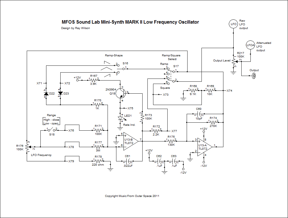
Schematic Page 7 Sound Lab Mini-Synth Mark II Low Frequency Oscillator
View as PDFThe LFO is a simple two op amp circuit that is comprised of an integrator and a comparator. The direction of the integrator's ramp is controlled by the comparator's output which is fed back to the comparator's input. It ramps down when the comparator's output is high and ramps up when the comparator's output is low. The rate is controlled by the amount of current arriving at the comparator's input. Diodes can be switched in or out of the feedback network to change the shape of the LFO's waveform.
Op amp U13-B in conjunction with C61 forms an integrator. The current into the integrator's input comes from the output of U13-A which is used as a comparator whose threshold is set at ground but whose hysteresis (set by R174 270K resistor) is such that the non-inverting input voltage level has to go well above ground to get the output to go high and well below ground to get the output to go low. C60 helps to square up the output of the comparator. If S16 (Ramp Shape) is in the center off position, S18 (Range set) is open, S17 (Ramp/Rect Select) is in Ramp position and the output of U13-A is low (negative saturation voltage of about -11V) the low level present on U13-A's output is applied to one side of adjustable voltage divider R176 (100K LFO Frequency pot). The voltage at the wiper of R176 is converted to current via R177 into the integrator. Since the voltage is below ground the integrator's output ramps up. U13-B attempts to keep the same voltage on it's inverting input as is present on the non-inverting input by pumping current through C61 as it ramps up linearly. When the voltage ramps high enough to overcome the hysteresis of U13-A (about 5V) the output of U13-A snaps high and now a high level (U13-A positive saturation voltage, about 10.5V) is present at the top of adjustable voltage divider R176 and the picked off voltage at the wiper is again converted to current and causes the integrator to ramp down until the voltage on the comparator's non-inverting input is low enough to cause it to snap low (about -5V) and the cycle repeats resulting in oscillation.
When in rectangle mode (S17 in the Square position) the same thing takes place with the only difference being that the path back to the integrator's input via S16 in either non-center position is opened so that the square wave is independent of the setting of the ramp shape. When in ramp mode (S17 in the Ramp position) the setting of S16 determines the ramp shape. The shape can be triangular (S16 in the center off position), ramp (S16 in the ramp position) or sawtooth (S16 in the sawtooth position). In triangle mode the current pulled through R177 is equal in both directions thus the integrator ramps up and down at approximately the same rate. When S16 is in either non-center position the current is greatly increased in either the positive or negative direction depending on which diode is put into the feedback path. With D22 in the path when the comparator goes low the current through D22 and R170 (1K resistor) causes the integrator to go high rapidly. With D23 in the path when the comparator goes high the current through D23 and R170 (1K resistor) causes the integrator to go low rapidly. The ramp and sawtooth waves oscillate at about twice the frequency of the trianglular waveform since one half of the wave is essentially removed.
When S18 is closed (High Range) the current into the integrator is multiplied by about 10 and thus the LFO's frequency range goes up by a factor of about 10. The triangle wave output is current limited via R172 and the square wave present on the output of U13-A is attenuated to a little less than half of it's -11V to +10.5V range or +/-5V. The output taken from S17 is applied to one side of adjustable voltage divider R217. The attenuated level set by the LFO Output level pot is sent to the VCO modulation switches. The unattenuated output of the LFO is applied to the VCF and VCA modulation level set pots. The attenuated level is also fed to the panel mounted banana jack for patching to the Sample and Hold input or other modulation inputs.
LED1 glows when the output of the integrator goes high enough to turn on Q18 which then allows current to pass through and light it indicating the rate of the LFO. In high range the LED may appear to glow constantly at high LFO rates. In low range the LFO's frequency can be adjusted between 0.02 Hz to about 7 Hz. In high range the LFO's frequency can be adjusted between 0.5 Hz to about 225 Hz.
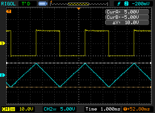
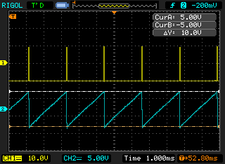
LFO Scope Photos
Settings are shown in the first cell and then only the changes are shown.
|
|
|
|
|
|
|
|


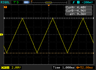


Schematic Page 8 Sound Lab Mini-Synth Mark II Voltage Controlled Amplifier
View as PDFThe VCA is built around U14-A a LM13700 transconductance amplifier. It is linear in response to control voltage. U15-A serves as an inverting control voltage summer and mixes the voltages arriving at it's inverting input. U15-A's output is fed to U15-B wired as an inverting unity gain buffer which reinverts the polarity of the mixed control voltages. U15-B's output is fed to the resistive divider comprised of R190 and R191. R190 is connected to -12V and holds the junction of the two resistors at a negative voltage which keeps U14-A from passing a signal through. Applying a positive voltage to the inputs of U15-A biases the junction of R190 and R191 up so that as the input voltage is increased U14-A begins to pass the signal on it's input to it's output (the transconductance of the op amp rises). C64 capacitively couples the output of the VCF into the VCA so as to get rid of any DC offset from the VCF. The output of the VCA is capacitively coupled to the R196 100K audio taper Master Volume pot. The resistors R195 and R194 set the gain and bias levels around the LM13700 transconductance op amp.
The biasing of the control for the VCA's AD Envelope Generator modulation level (R185 100K pot) set by R187 and R188 is such that when it is turned all the way down the VCA is on. As R185 (VCA AD Modulation) is advanced clockwise the modulation provided by AD Envelope Generator 2 is more and more pronounced. The other modulation control for the VCA (R179 100K pot) permits the VCA to be modulated by either the LFO or VCO1. When S19 is in the center off position regardless of which of the modulation sources is selected no modulation is applied. When either source is selected via S19 advancing R179 (VCA Modulation) control increases the modulation provided by the selected source.
VCA Scope Photos
Settings are shown in the first cell and then only the changes are shown.
|
|
|
|
|
|
|


Schematic Page 9 Sound Lab Mini-Synth Mark II Sample & Hold
View as PDFThe sample and hold circuit is built around a single quad op amp (LF444). The LF444 has the characteristics necessary to allow the sampled voltage to remain on the sample cap a relative long time due to it's incredibly high input impedance and super low input current. It works far better than other JFET input amplifiers in this application.
The circuit consists of two parts, the sample clock generator and the sampling section. The sample clock is the same type of oscillator as is used in the ADEG Repeat Gate Generators. So I won't describe the whole operation only the differences between it and them. The range is a bit different due to the 10uF timing cap instead of the 4.7uF cap of the Repeat Gate Generators. This allows the sample and hold sample clock to run slower than the ADEG Repeat Gate Generators. Another difference is the 1N914 diode D25 in the timing capacitor charge path. The diode circumvents R212 the 1M Sample Rate pot so that when the output of U16-D is high C74 is rapidly charged via forward biased 1N914 diode D25 and R211 4.7K resistor. When U16-D's output is low the capacitor discharges at the rate set by R212 Sample Rate pot. The purpose of the diode is to cause the output of U16-D to be a positive going rectangular pulse wave instead of a square wave. This pulse wave output (point X91) becomes the trigger output that is sent to the ADEGs via the normalized switching arrangement. The front edge of the pulse at the output of U16-D is fed via C71 (100pF cap) to be dropped across R207 in parallel with D24. This differentiated pulse is tied to the gate of Q19 2N5457 sample switch JFET via R199 (100K resistor). The gate is also tied to -12V via R200 (470K resistor). The source to drain of Q19 is essentially open circuit when Q19's gate is held at -12V by R200. The narrow pulse applied to the gate during the sample clock's low to high transition causes Q19 to turn on momentarily (essentially shorting source to drain) allowing the voltage that is on the output of U16-A to charge or discharge capacitor C68 (.005uF polystyrene). C68 should be polystyrene or similatr low leakage capacitor so that the sampled voltage does not leak away due to internal capacitor leakage. Polystyrene caps are very low leakage and temperature stable although the temperature stability is not a critical factor in this circuit (as it is in the VCOs).
The voltage applied to the input via attenuator R210 is cut in half by resistive divider R197 and R198. The level of the signal is shifted up due to the biasing on the inverting input via R201 connected to -12V so that the voltage applied to the source of Q19 is always above ground. The voltage on the sample cap is presented to the non-inverting input of U16-B. It is very critical that U16 be a JFET ultra low input current op amp so that the sample does not droop significantly. It will droop a bit and at low sample rates this may be audible when modulating the VCOs or VCF. At sample rates above 1Hz the droop will be undetectable. U16-B also provides gain and offset to the signal to restore it to it's original levels (above and/or below ground). The gain is added so that you can really modulate the VCOs and VCF over a wide range with the sampled voltage. The overall range of the Sample & Hold's output is set by the input attenuator. As you increase the input level by advancing R210 (Input Level pot) you can go from the condition where the output levels of the sample and hold are lower than the input signal levels to the point where the output levels are higher than the actual input signal level.
The output of U16-B is fed to the end of the R209 1M Glide pot. The pot is wired as a variable resistor and sets the slew rate of how fast C75 (.1uF cap) is charged and discharged. R208 sets the minimum Glide time and Glide is undetectable when Glide is set to 0. As the Glide pot is advanced clockwise the voltage on the output of U16-C slews from level more and more slowly. U16-C feeds the Sample & Hold output banana jack which allows patching to other modulation inputs. The Sample & Hold output is also normallized for connection to the VCOs via switching. The VCF has an extra CV input banana jack for modulation by external sources including the Sample & Hold for some very cool VCF modulation effects.
R118 must be trimmed to set the output voltage to 0V when ground is applied to the input of the sample and hold (Input Level pot is turned all the way down).

Sample & Hold Scope Photos
Settings are shown in the first cell and then only the changes are shown.
|
|
|
|
|
|

Sound Lab Mini-Synth Mark II Calibration
The signal to be observed and measured during VCO and VCF calibration is the output of the synthesizer, thus the Master Volume should be turned fully on during the calibration procedure. Other test points will be specified as necessary.
Please read over the entire procedure before beginning so you know what's coming up next and what results to expect.
VCO Scale Calibration
Both VCOs need to be calibrated so that the scale factor is correct (1V/octave). You will need an accurate DVM and a frequency counter. In lieu of a frequency counter your ears or another keyboard can be used to determine when each oscillator is correctly "tuned". You will also need an accurate voltage source. An analog keyboard controller or MIDI to CV module that is in good calibration is the best. You will need to be able to apply at a minimum 0,1,2 and 3 volts with an accuracy of +/-2mV at least.
For example:
- at the 0V setting you will want your DVM to read between -.002V and +.002V,
- at the 1V setting you will want your DVM to read between +0.998V and 1.002V,
- at the 2V setting you will want your DVM to read between +1.998V and +2.002V,
- at the 3V setting you will want your DVM to read between +2.998V and +3.002V.
The closer to the ideal (0.000, 1.000, 2.000 and 3.000) the better.
Each voltage controlled oscillator has both a 100 ohm scale adjust trimmer (VCO-1 -> R49, VCO-2 -> R88) and a 100K high frequency compensation trimmer (VCO-1 -> R43, VCO-2 -> R82). I will describe the calibration procedure for VCO-1. The same procedure will be used for all VCOs but, of course, using each oscillator's respective trimmers.
Only one LOG-CV input should be applied to each VCO during calibration and all other inputs to the VCO should be disconnected (i.e. remove any connected banana cables from the jacks). At the start of the calibration procedure for each oscillator the high frequency compensation trimmer should be set so that the maximum resistance is between pins 3 and 2. At this setting the pot has the minimum effect on the VCO's V-to-F response. You can determine the direction to turn the trimmer by listening to the oscillator being calibrated at about 2KHz and adjusting the high frequency trim. If the frequency starts to decrease slightly you are turning it in the correct direction, if the frequency starts to increase turn the trimmer the other direction. Adjust the trimmer until you hear or feel end of travel clicks.
- Let the synth acclimate to the room's temperature under power for at least half an hour before beginning the procedure.
- Connect the Keyboard Control CV input to your control voltage source.
- Select KBD for both VCO modulation controls.
- Turn all mixer inputs fully counter-clockwise (off).
- Turn the VCF initial cut-off frequency fully on.
- Turn the VCF resonance fully off.
- Turn the VCA ADEG Modulation all the way counter clockwise.
- Turn all VCF and VCA modulators all the way counter clockwise.
- Turn the mixer input for VCO-1 fully clockwise (on).
- Apply 0 volts to the Keyboard Control CV input.
- Use VCO-1's coarse and fine frequency controls to set it's frequency to 100 HZ.
- Increase the voltage being applied to the Keyboard Control CV input to 3 volts.
- The scale adjust trimmer will need to be adjusted to achieve a change of from 100 Hz to 800 Hz when the voltage is increased.
- Tweak the scale adjust trimmer while you alternate the voltage being applied to VCO-1's LOG-CV input between 0V and 3V until the change in frequency is correct.
- Use VCO-1's coarse and fine frequency controls to set it's frequency to 800 HZ.
- Apply 0 volts to the Keyboard Control CV input.
- Increase the voltage being applied to the Keyboard Control CV input to 2 volts.
- The scale adjust trimmer and the high frequency compensation trimmer will need to be adjusted to achieve a change of from 800 Hz to 3200 Hz when the voltage is increased.
- Tweak the scale adjust trimmer and the high frequency compensation trimmer while you alternate the voltage being applied to VCO-1's LOG-CV input between 0V and 2V until the change in frequency is correct.
Repeat the procedure for each of the VCOs adjusting their respective trimmers. Remember to turn the mixer channel for the oscillator you are tuning up and the others down. You will REALLY be mad if you spend 30 minutes adjusting VCO-1 and then when you start calibrating VCO-2 you BY MISTAKE turn VCO-1's trimmers AGAIN!!!. So maybe put a sticky note over them or something to avoid this time consuming disaster (don't ask me how I know this). When all is said and done each VCO should respond so that each change in 1V applied to it's LOG-CV input results in a change in frequency of 1 octave.
This procedure is iterative, the adjustments are sensitive and the trim pots are somewhat interactive. Be prepared to take your time doing this and know that what I have described is the "ideal". You will finally arrive at a tradeoff in which the lower octaves are more in tune than the upper ones but with careful adjustment you will be able to achieve a very in tune musical range 20Hz to 2560Hz for the VCOs. With careful adjustment even higher registers can be scaled properly.
YouTubes about oscillator calibration in general...
VCF Scale Calibration
The Sound Lab Mini-Synth Mark II's State Variable VCF will oscillate when the resonance control is advanced to maximum. The waveform is a very nice sine wave when the filter is set to "Low Pass" filter shape (Band Pass has a slight distortion). You can adjust the VCF's V-to-F response so that the oscillator tracks 1V/oct over a limited range. To do so follow this procedure.
- Let the synth acclimate to the room's temperature under power for at least half an hour before beginning the procedure.
- Connect the Keyboard Control CV input to your control voltage source.
- Turn all mixer inputs full counter-clockwise (off).
- Turn the AR MOD and LFO-1 MOD for the VCF all the way off (counter clockwise).
- Turn KBD Switch for the VCF on (to KBD).
- Apply 0 volts to the Keyboard Control CV input (disconnect the other EXT-CV input (i.e. remove any connected banana cable from the other jack)).
- Turn the VCF's Resonance control fully on.
- Use the VCF's Coarse and Fine Cutoff Frequency controls to set it's frequency to 100 HZ.
- Increase the voltage being applied to the the Keyboard Control CV input to 2 volts.
- The VCF's 100 ohm scale adjust trimmer R280 will need to be adjusted to achieve a change of from 100 Hz to 400 Hz when the voltage is increased.
- Tweak the scale adjust trimmer while you alternate the voltage being applied to VCF's EXT-CV input between 0V and 2V until the change in frequency is as close as possible to this ideal.
- Apply 0 volts to the Keyboard Control CV input.
- Use the VCF's Coarse and Fine Cutoff Frequency controls to set it's frequency to 320 HZ.
- Increase the voltage being applied to the the Keyboard Control CV input to 2 volts.
- Tweak the scale adjust trimmer and the high frequency compensation trimmer while you alternate the voltage being applied to VCO-1's LOG-CV input between
0V and 2V until the change in frequency (320Hz to 1280Hz) is correct. Go back and recheck the previous frequency response.
This procedure is iterative, the adjustments are sensitive and the trim pots are somewhat interactive. Be prepared to take your time doing this and know that what I have described is the "ideal". You will finally arrive at a tradeoff in which the lower octaves are more in tune than the upper ones but with careful adjustment you will be able to achieve a very in tune musical range 20Hz to 1280Hz for the VCF. With careful adjustment even higher registers can be scaled properly.
Noise Amplitude Adjustment
The Sound Lab Mini-Synth Mark II's White Noise Generator has an amplitude trimmer which should be adjusted for proper white noise amplitude. Just a note on noise. I have found that selected 2N5172 transistors produce excellent noise. I bought 1000 of them and have found that about 1 in 5 produce high quality high amplitude noise. While selected 2N3904 transistors will produce good noise if you like you can purchase pre-selected 2N5172 noise transistors from me. Just make sure you install the transistor into the board in the correct orientation so that the emitter and base pins are oriented properly. The collector should be removed.
- Observing U9 pin 7 (output of the noise generator) with an oscilloscope (10mS per div and 2V per div).
- While observing U9 pin 7 adjust R123 100K trimmer until the amplitude of the observed noise signal until the maximum noise peaks are within +/-5V.
Sample & Hold Offset Null Adjutstment
The Sound Lab Mini-Synth Mark II's Sample & Hold module needs to have it's output offset nulled by adjusting trimmer R118.
- Turn the S&H Input level control to 0 (completely counter-clockwise).
- Adjust 100K trimmer R118 until the output of U16 pin 7 is as close to 0 volts as possible.