Ray Wilson authored this content while he was actively running MFOS as the founder and resident genius.
We retain the content because it reflects a valuable point of view representing that time and place.
Article by Ray Wilson
While trouble shooting an issue I discovered a problem related to reverse bias on tantalum capacitors. When tantalum caps are exposed to reverse bias they develop leakage leading to eventual failure. A few circuits use tantalums where non-polarized aluminum caps would be a better choice. I have looked over all of the MFOS circuits and identified a small number of circuits where this may result in a problem. This circuit is one of the affected designs. I have not had any reports from the field regarding this and discovered it when my ULTIMATE's sample and hold clock started acting oddly.
If you start to see the sample and hold clock stop working when setting the pot to lower settings I recommend that you change C64 (2.2uF Tantalum Capacitor) to a 2.2uF non-polarized aluminum capacitor. Even though the voltage on C64 oscillates about ground it spends a majority of its time between ground and -2.5 volts. This results in C64 becoming leaky and preventing the sample clock oscillator from oscillating at lower settings. The part list has been updated to reflect this.
If you start to see the repeat gate stop working when setting the pot to lower settings I recommend that you change C69 (10uF Tantalum Capacitor) to a 10uF non-polarized aluminum capacitor. The voltage on C69 oscillates about ground which causes C69 to see negative voltage about 50% of the time. This results in C69 becoming leaky and preventing the repeat gate oscillator from oscillating at lower settings. The part list has been updated to reflect this.
THE PC BOARD LEGENDS FOR C64 and C69 HAVE POLARITY MARKINGS. IGNORE THEM WHEN INSTALLING THE NEW NON-POLARIZED CAPS
The Sound Lab ULTIMATE has a normallized signal path for all of the sound sources through the MIXER, VCF and VCA. The VCF and VCA have normallized modulation from the AR generator and the LFOs. You can easily route things differently with all of the available patch points.
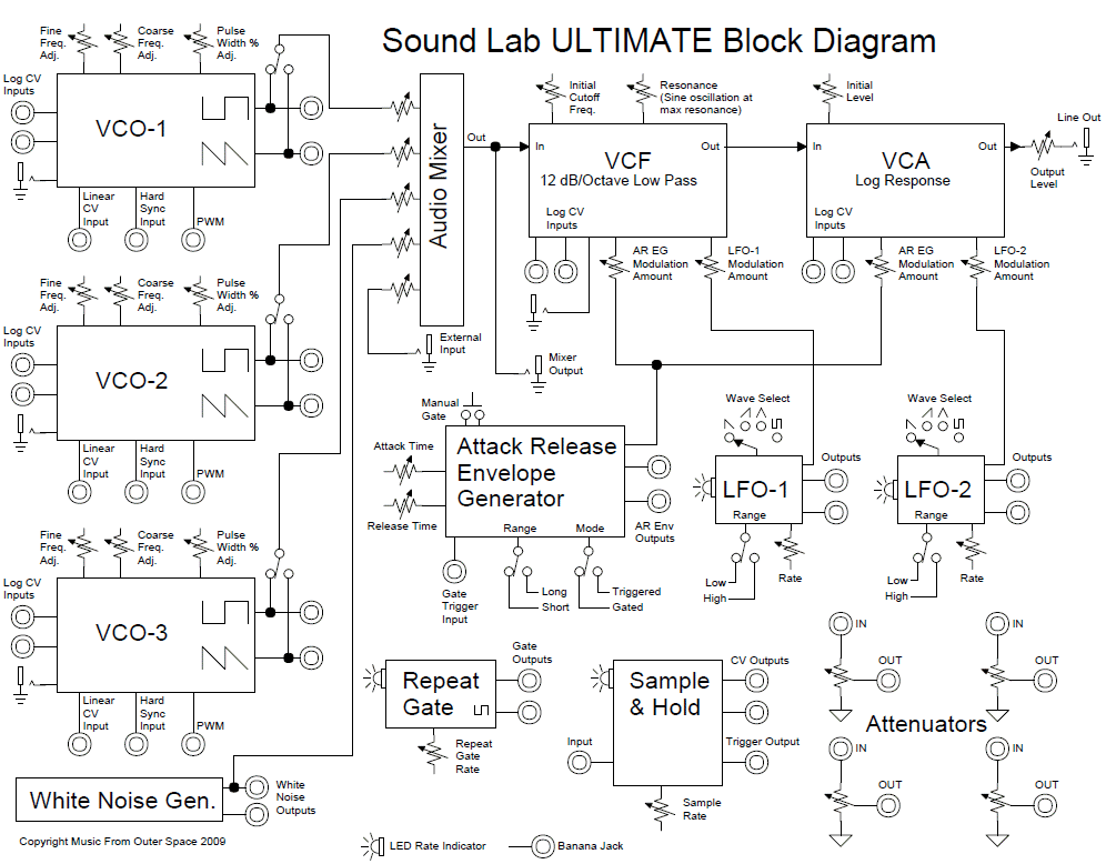
Circuit Description
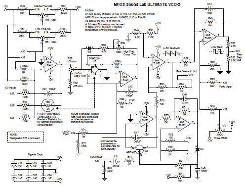
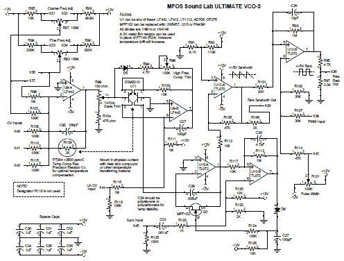
The Sound Lab ULTIMATE has three identical VCOs. I will provide a description of VCO-1. The other VCO schematics differ only by component designators. Inputs and outputs are arranged the same as for VCO-1 and differ only in Xn number. Each oscillator provides well over 6 octaves of excellent in-tune tracking and features sawtooth and variable width rectangular waveform outputs. These waveforms in conjunction with low pass filtering via the VCF provide a wealth of timbres. The VCOs are ramp-core type.
Six voltage inputs (five exponential (X5, X7, X10, X11 and X13) and one linear (X14)) control the frequency of each oscillator. Two of the CV inputs (X5 and X7) are wired to the Coarse and Fine Frequency Adjust pots (R3 and R6 respectively). The other control voltage inputs (X10, X11 and X13) are wired to the banana and 1/4" jacks on the front and auxiliary panels (see the wiring diagram section). These pots are wired as variable voltage sources. The coarse pot provides between about -10V and +4.5V which is fed via the wiper of R3 to voltage summer (op-amp U1-A) input resistor R12. That's a lot of coarse adjustment (14 octaves). The coarse pot will adjust the frequency from a few Hz to about 20 kHz. The fine pot provides between -2.4V and +2.4V but since it is fed into the voltage summer via R10 (1 meg ohm) it only changes the frequency of the oscillator a few semi-tones from min to max adjustment.
The voltage summer provides a gain of -.02 for the inputs with 100K input resistors and -.002 for the fine input which has a 1M input resistor. Thus a change of 1V applied to an input with a 100K input resistor results in a change of -20mV at U1-A's output. A change of 1V applied to an input with a 1M input resistor results in a change of -2mV at U1-A's output. Since the voltage needed to double the current in the linear V to exponential I convertor is about -18 mV R11 provides adjustment to scale U1-A's output to the correct voltage per volt of input. This trimmer is adjusted later to scale the oscillators to precisely 1V per octave.
U1-B in conjunction with U3 (SSM2210 matched NPN transiator pair) comprises a linear voltage to exponential current convertor. The NPN transistor in the feedback loop of U1-B (U3 pin 6-e, 7-b, and 8-c) is responsible for this remarkable effect. For further reading and explanation of exponential convertors see National Semiconductor Application Note 30 "Log Convertors" by Robert C. Dobkin and Musical Application Of Microprocessors Second Edition by Hal Chamberlin Chapter 6 "Basic Analog Modules"
In this configuration the voltage applied at the base of the NPN transistor (U3 pin 7) controls the current that flows into the collector of the NPN transistor (U3 pins 1-c, 2-b, and 3-e). The relationship of voltage to current is exponential. For every increment of -18mV at the base of the transistor (U3 pin 6-e, 7-b, and 8-c) the current flowing into collector (U3 pin 1) doubles in magnitude. The low end of the range of current that this circuit provides starts at about .02uA when both the coarse and fine pots are turned fully counter-clockwise. When the coarse pot is adjusted to about 40 Hz the current is at .4uA and doubles for every octave thereafter (80 Hz .8uA, 160 Hz 1.6uA, 320 Hz 3.2uA, 640 Hz 6.4uA, 1280 Hz 12.8uA, 2560 Hz 25.6uA, etc.). R16 sets the initial current for U1-B's feedback loop (1.2uA). By applying control voltage to R22 1M resistor this current set is affected directly and thus input X14 provides a linear frequency modulation input. C6 stabilizes U1-B since it is not at unity gain.
A metal film 2K Ohm 1/4W +/-2% T.C. +3300 PPM tempco is used as the feedback resistor around voltage summer U1-A. This TC is used to cancel out the exponential convertor's temperature coefficient. If a metal film resistor is used in it's place the oscillators will drift quite a bit more with temperature changes. The ideal compensation is about 3300 PPM. The Precision Resistor Company writes this about their 3500 PPM compensators. The actual TCR of a standard 3500 element is very close to +3350 ppm/°C. at 25°C. and lower than +3450 ppm/°C. at 100°C. So these compensators work quite well. D1, R7 and 100K trimmer R8 are used to compensate for the bulk emitter resistance of the base emitter junction. This resistance causes the oscillator to go flat at higher frequencies. Adjustment of R8 allows this error factor to be compensated so that the oscillator works over a wide range of frequencies.
The current flowing into collector U3 pin 1 controls the frequency of the VCO. Op amps U2-A and U2-B in conjunction with Q1 MPF102 N-Channel JFET form the heart of the ramp-core oscillator. U2-A is used as an integrator in association with C7. Current flowing out of U2-A pin 2 into collector U3 pin 1 causes U2-A pin 1 (U2-A's output) to rise linearly in voltage. This is because U2-A's output is trying to hold pin 2 at the same potential as pin 3 which is connected to ground. U2-A's output is connected to U2-B which is wired as a comparator. When the voltage at U2-A pin 1 rises above the threshold set by R23 and R26 (slightly above two volts due to the hysteresis provided by R18) U2-B's output (which had been sitting at about -10.5V) shoots to +10.5V. When that happens Q1's gate is brought high (via D2 and R28) which essentially shorts it's drain to source discharging C7 (.005uF polystyrene or polycarbonate) integrator capacitor and resets the integrator's output to ground. Since the voltage on U2-B's non-inverting input is now below the threshold set by R23 and R26 it's output returns low (-10.5V) and U2-A's output begins to ramp up again and the cycle continues resulting in ramp wave oscillation. C5 conducts the rising output of U2-B to it's non-inverting input (positive feedback) in order to make sure the output snaps high quickly and completely. The pulse that occurs on the output of U2-B forward biases D2 and charges C2 100pF cap. This charge insures that Q1 stays on long enough to completely discharge C7. U2-B's output returns low so fast that without this additional charge to keep Q1 on C7 would not be discharged effectively.
Thus the output of U2-A is a ramp wave whose frequency is directly proportional to the current flowing out of U2-A pin 2. Op amp U4-A level shifts and inverts the ramp causing it to become a +/-5V sawtooth wave oscillating about ground. U4-A's output is fed to the front panel connections (X8) via 3K to protect it from being directly shorted to something it would not like.
The sawtooth waveform is fed into the non-inverting input of U4-B wired as a comparator via R34. When the sawtooth is above the voltage seen at U4-B pin 6 (plus a bit of hysteresis due to R35) the output of U4-B goes high. When the sawtooth is below the voltage seen at U4-B pin 6 (plus a bit of hysteresis due to R35) the output of U4-B goes low. Pulse width adjustment pot R39 (100K) sets the voltage level on U4-B pin 6 (via 47K at X12) and thus changes the duty cycle of the rectangular pulse appearing on U4-B's output. External pulse width modulation input is via R37 at X9 (20K resistor) which is connected to the front panel banana jack. R40 and R41 reduce the amplitude of the rectangle wave to +/-5V and R40 doubles as U4-B's output protection resistor (to point X6) to protect it from being directly shorted to something it would not like. C11 sharpens up the rectangular waveform by applying positive feedback for the edge of the output back to the non-inverting input. I do this regardless of what the chip spec says about it's intrinsic output protection.
The sync input (X15) permits another oscillator to cause this oscillator to reset prematurely. The other oscillator must provide a hard edge to effective sync this oscillator (rectangular, saw or ramp). When the other (sync source) oscillator is oscillating at a lower frequency than this oscillator and this oscillator is swept low to high a distintive timbre is produced by this oscillator.
| Sound Lab ULTIMATE VCO-2 | Sound Lab ULTIMATE VCO-3 |
 |
 |
Sound Lab ULTIMATE Audio Mixer Table Of Contents
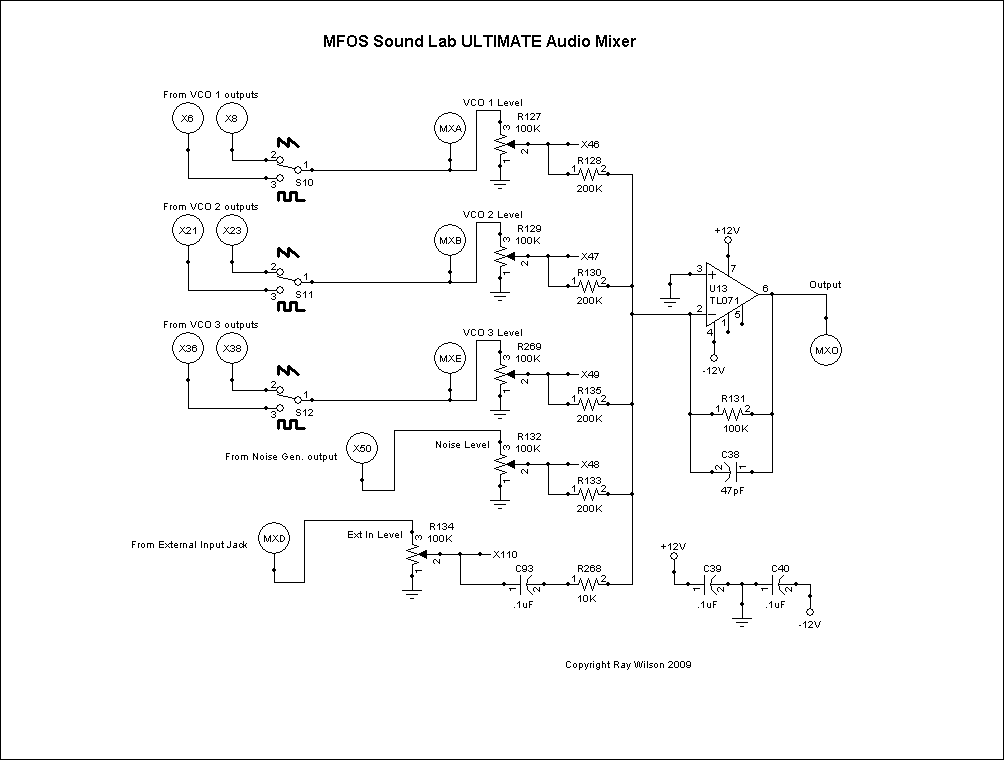
Circuit Description
This is a simple active mixer built around the U13 TL071 low noise op amp. It provides adjustable levels for the three VCOs, the noise source, and the external input. The synth signal inputs get a gain of .5 because they are fed in via 200K resistors and the mixer's op amp (U13) has a feedback resistor of 100K. The external input has the potential for a gain of 10 when the pot is turned completely up. So the external signal source should have a level of around +/- 500 or 600 mV.
The advantage of an active mixer is that the input node (pin 2 of U13) is a virtual ground. Thus the inputs act more independently because there is very little to no interaction between the volume level settings. This is an inverting mixer.
If you are familiar with op amp operation then you know you can, of course, pick other values for the oscillator and noise input mixing resistors (R128, R130, R135 and R133) as well as the op-amp's feedback resistor R131 so that the mixer can give more gain to the external input or white noise if you want it to. For example if all of these resistors (R128, R130, R135, R133 and R131) were multiplied in value by 10 (2M for the 200K resistors and 1M for the 100K feedback resistor) then the external input would have the potential for a gain of 100 which may be more useful for, say an electric guitar.
I added C38 to stabilize the operation of op-amp U13. Op-amps are generally compensated for unity gain and when the gain is higher or lower than that I add the compensation capacitor for good measure.
The pots are wired to the VCO wave selector switches as part of the panel wiring. I ran twisted pair from the pots to the board. There are ground connections on the PCB near the input resistors for connecting either the shield from coax or the the ground wire if you use twisted pair. I only grounded the PCB side of the twisted pairs. The mixer's output (circuit point MXO) is connected to the input of the VCF.
Sound Lab ULTIMATE Noise Generator Table Of Contents
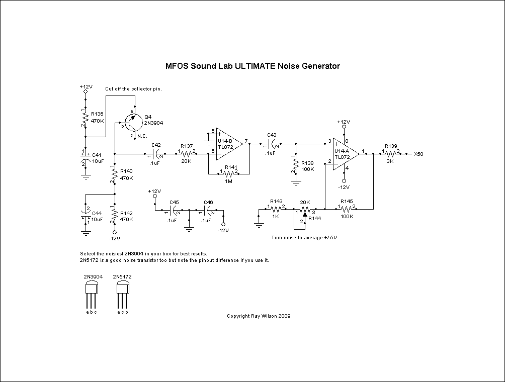
Circuit Description
The goal of this noise generator design was to keep as much circuit noise out of the noise generation portion as possible. Keeping noise out of noise might sound odd but when the noise generator is polluted by cyclic sources like oscillators, 60 cycle hum, or other line noise the purity of the noise can be affected. No one likes wind sound with 60 cycle hum in it.
Thus 470K resistor R136 goes from +12V to both the emitter of the transistor and a 10uF capacitor to ground. This insures that the voltage sitting at that junction is quiet and protected from sources of cyclic supply noise. The base is then connected to a 470K resistor R140 that also goes to a 10uF cap that is isolated from the negative supply by 470K resistor R142. The noise signal results from the reverse biasing of the emitter base junction to a level beyond it's advertised V-EBO (emitter base breakdown voltage). This results in an avalanche effect in which electrons cascade across the junction banging into one another and making a teeny tiny little racket which we amplify the heck out of.
The actual noise signal is generated at the junction of Q4's base and 470K R140. The low level noise signal is coupled into the first gain stage via C42 and R137. A gain of 50 is achieved by op-amp U14-B whose output is fed into U14-A via C43 where it is amplified further. Trimmer R144 is used in the gain set of U14-A so that the noise level can be trimmed to about +/-5 volts.
Test several 2N3904s to find the noisiest one. You should be able to have the trimmer at about mid-way when you have a suitably noisey transistor. I put a note on the schematic that states that 2N5172 can be used just as well but note the pin-out difference and make sure you insert it into the board so the the emitter and base are oriented correctly related to how the 2N3904 would be inserted.
I bought a bunch of 2N5172 NPNs and found that about one in 8 of them stands TALL above the rest as far as noise generation. They are cheap and buying a bunch of them should net you a lot of really good noise transistors. You can find them here Synthfool's Parts. You will find less variation among the 2N3904s but I still encourage you to buy several (they are also very inexpensive) and then select the best of them. The noise signal is connected to the front panel connections via 3K protection resistor R139.
Sound Lab ULTIMATE VCF Table Of Contents
Circuit Description
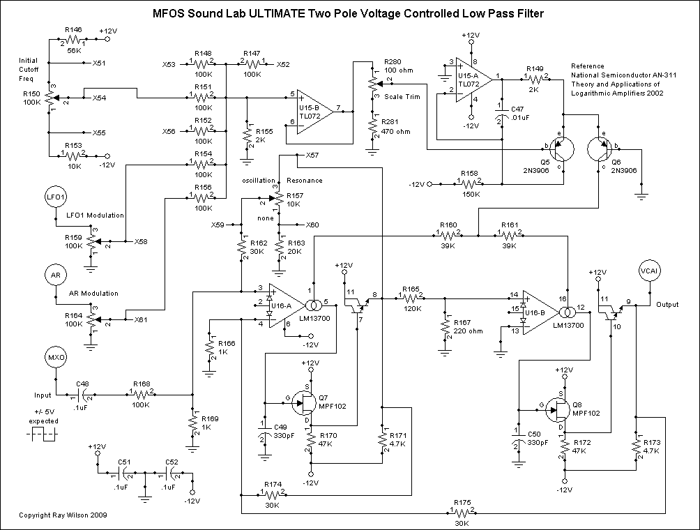
This VCF is a variation of the state variable filter design found in the Sound Lab but in this product only the lowpass output is available. This design provides plenty of resonance up to and including being a decent sine wave oscillator when the resonance control is advanced toward maximum.
The control voltage mixer and voltage to exponential current convertor are built around U15 TL072 Dual Op Amp. The control voltage mixer is non-inverting and mixes the CV inputs via 100K resistors onto a 2K resistor to ground (R155). This is a passive mixer but the 50 to 1 ratio of input resistor value to ground node resistor value is high enough that there is little interaction between the control voltage inputs.
Six CV inputs are provided. Three are hard wired: one (X54) to the Initial Cutoff Frequency pot, one (X58) to LFO-1 via a potentiometer wired as a voltage divider (R159) and one (X61) to the output of the Attack Release generator via a potentiometer wired as a voltage divider (R164). Two are brought to the front panel as banana jacks (X52 and X53) and one is connected to the quarter inch jack on the auxiliary panel (X56). This arrangement provides for endless combinations of modulation of the filter's cut off frequency.
This op amp saving design yields impressive results. The output of U15-B is adjustable via trimmer R280 thus the voltage can be scaled to +18mV per volt of control voltage input. Since the LM13700 requires positive current to flow into it's amp bias inputs PNP transistors are used in the linear voltage to exponential current convertor. (See "Musical Applications Of Microprocessors, Second Edition" by Hal Chamberlin 1985 pages 204 and 205) The control voltage mixer (U15-B) supplies +18 mV per increase of 1 volt of control voltage (after trimming R280). For every increase of 18mV applied to the base of Q5 there is a doubling in the magnitude of current flowing from the collector of Q6 into the amp bias inputs (via current limiter/splitters R160 and R161). I have had people write and say you don't need R160 and R161 but I would rather protect the sensitive amp bias inputs than be sorry because start-up and shut-down conditions are not always as friendly as powered up and operating normally conditions. I have never lost an LM13700 in circuit.
The two halfs of U16 (LM13700 Dual Transconductance Amplifier) are used as voltage controlled integrators in the filter circuit. This is an improvement on the state variable filter design found in the "National Semiconductor data sheet "LM13700/LM13700A Dual Operational Transconductance Amplifiers with Linearizing Diodes and Buffers" November 1994 figure 14. Source followers (Q7 and Q8) are added to the circuit to increase the impedance of the amplifiers that follow the integrators (U16-A and U16-B). This results in more accurate integration and the ability to oscillate when the Resonance control is advanced toward it's maximum level.
R280 permits the filter to be tuned to track close to one octave per volt of CV input.
The output of the filter is fed directly to the input of the VCA.
For a complete explanation of state variable filter operation see Programmable State-Variable Filter Design For a Feedback Systems Web-Based Laboratory by Rayal Johnson February 17, 2004
Sound Lab ULTIMATE VCA Table Of Contents
Circuit Description
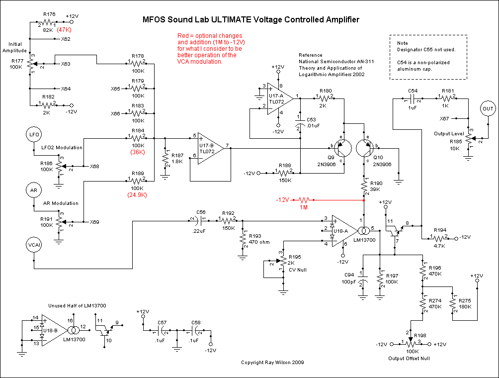
This is a very simple but effective log response VCA. The control voltage to expo current convertor is practically a clone of the VCF's expo circuit. Again positive current is provided to the amp bias input of a LM13700. As the transconductance through the amp increases via increasing control voltage (converted to current via the expo convertor) the signal fed into the input grows in amplitude at the output. The current through the LM13700 is converted to voltage by the built in buffer amp (onboard darlington pair) and fed to the output.
In a manner similar to the VCF the VCA is hard wired to control voltage from the Initial Amplitude pot, the Attack Release generator and LFO-2. Two CV inputs are brought to the front panel banana jacks (X65 and X66).
The CV null should be adjusted while modulating the VCA with LFO-2 set on square wave and all inputs of the mixer turned off. Adjust R195 2K trimmer until the output of the VCA (U18-A pin 8) is at a minimum (it should trim to less than 5 mV of CV feedthru). Adjust R198 100K trimmer for minimum offset at the output of the VCA (U18-A pin 8). Adjust R198 to get the output of the VCA (U18-A pin 8) as close to ground as possible.
The output of the VCA is fed to the synth's output jack via C54 (non-polarized 1uF cap) and R181 (1K resistor).
While looking over an ULTIMATE for a customer recently who felt that the VCA modulation was not performing as he would like I adjusted some of the values on the VCA which improved the operation IMHO. These changes are optional and as always if you are happy with the VCA modulation as it is, not necessary at all. I made these changes to my ULTIMATE and I like it better myself. With these changes you don't need to turn the initial level up as much in order for the AR and LFO modulation to effect the amplitude. I also noticed that the LFO modulation is superceded by the AR modulation (which I also like).
- R176 changed from 82K to 47K.
- R184 changed from 100K to 36K.
- R189 changed from 100K to 24.9K.
- Added a 1M resistor from U18-A pin 1 to -12V.
The last change (adding a 1M resistor from U18-A pin 1 to -12V) is not hard and I did it by soldering the 1M resistor between the leg of R190 (39K) which goes to U18 pin 1 and the -12V side of C58. Image of optional kludge. The parts list still reflects the old values since these are totally optional changes but I would suggest them for new builds.
A builder (Peter Kvitek of Santa Clara, CA) let me know that after he had performed these mods he needed to change the CV Null trimmer from 2K to 10K. I left mine at 2K but if you have an issue with the CV Null you might give Peter's suggestion a go.
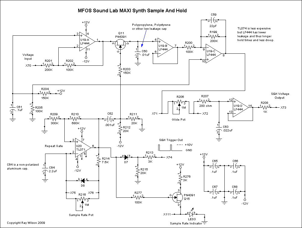
Sound Lab ULTIMATE Sample & Hold Table Of Contents
If you start to see the sample and hold clock stop working when setting the pot to lower settings I recommend that you change C64 (2.2uF Tantalum Capacitor) to a 2.2uF non-polarized aluminum capacitor. Even though the voltage on C64 oscillates about ground it spends a majority of its time between ground and -2.5 volts. This results in C64 becoming leaky and preventing the sample clock oscillator from oscillating at lower settings. The part list has been updated to reflect this.
THE PC BOARD LEGEND C64 HAS POLARITY MARKING. IGNORE IT WHEN INSTALLING THE NEW NON-POLARIZED CAP
Circuit Description
The Sound Lab ULTIMATE sample and hold section consists of a pulse generator (to turn on the sampling JFET and provide an output trigger) and the sampling section.
The pulse generator works as follows. Op amp U20 has R210 (680K resistor) applying positive feedback to it's non-inverting input (U20 pin 3). R209 300K resistor is connected from (U20 pin 3) to ground. On start-up U20's output might be high or low (it does not matter). We will consider the low on start-up case. When power is applied and U20's output is low (-11V) C64 (2.2uF non-polarized aluminum cap) who had been sitting at ground begins to charge toward -11V via R216 (1M linear potentiometer) wired as a variable resistor and R214 (7.5K resistor). D8 (1N914 diode) is reverse biased so current does not flow through it. Under this condition R210 and R209 form a voltage divider that holds U20 non-inverting input pin 3 at about -3.3V. Eventually C64 charges to below -3.3V at which time the non-inverting input of U20 sees a higher voltage than the inverting input. Now U20 acts like a comparator and it's output flips high (+11V). Now the voltage on the non-inverting input is held at about +3.3V (by voltage divider R210 and R209) and C64 begings to rapidly charge toward +11V via R214 (7.5K) and foward biased D8 (1N914 diode). As soon as C64 charges to above +3.3V U20 acts like a comparator and it's output flips low and the cycle repeats resulting in oscillation. D8 and R214 permit C64 to charge quickly when the output of U20 is high. When U20's output is low C64 discharges toward -11V via R216 and R214 (D8 is reversed biased). So R216 controls the rate of the sample clock oscillator and the output of R214 is a narrow positive going (-11V to +11V) pulse. The sample rate can be varied from approximately .5Hz to 50 Hz.
The input signal to be sampled is applied to R201 (200K resistor) which is the input resistor to op amp U19-A. U19-A inverts this input, applies a gain of 0.5 and offsets the resulting output signal to operate about a level of 6.5 to 7 volts. Sampling switch Q11 (N Channel PN4391 JFET ) provides a higher off resistance when in the hold state if the signal on it's source is kept above ground.
The front edge of the low to high pulse output of the sample clock generator (U20) is applied via differentiator C62 (.001uF cap) and bias network R211 (20K resistor) and R212 (20K resistor) resulting in a much narrower pulse. This pulse is applied via R203 (150K resistor) to the gate of N-Channel JFET Q11. This turns Q11 on, essentially shorting the source to drain so that C60 (.01 uF low leakage cap) can charge to the voltage appearing at the output of U19-A. This is the sampling state.
Once Q11's gate returns to the level applied by the junction of R211 and R212 (about -6V) Q11's source to drain resistance is equivalent to an open circuit (the hold state) and sample cap C60 has no path to discharge but into the high impedance non-inverting input of buffer U19-B (which is equivalent to 100s of M-Ohms).
The sampled voltage is re-inverted, given a gain of 2 to restore it to it's original amplitude and level shifted to operate about ground by op amp U19-C. The voltage at U19-C's output is fed to the output buffer U19-D via the glide pot (R206 1M pot wired as a variable resistor) and R207 (200 ohm resistor). The .022uF cap on the non-inverting input of U19-D in conjunction with R206 (1M pot) provides variable glide time (0 to 2 seconds) from sample to sample.
The input to the sample and hold (X70) is available on the front panel banana jack. The circuit can sample levels of between about -7V to +7V. The output (X73), a sampled reflection of the input, is fed to three banana jacks on the front panel. The trigger output of the circuit (X74) is fed to a banana jack on the front panel. The trigger output goes from ground (when U20 pin 6 is low and D7 is reverse biased) to about 10.5 volts when the sample pulse occurs and D7 conducts the positive excursion of U20's output and drops it on R215 (20K resistor). LED3 provides a visual indication of the sample rate on the front panel.
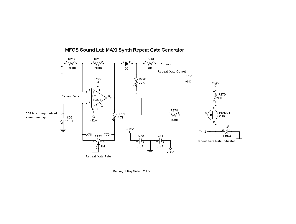
Sound Lab ULTIMATE Repeat Gate Generator Table Of Contents
If you start to see the repeat gate stop working when setting the pot to lower settings I recommend that you change C69 (10uF Tantalum Capacitor) to a 10uF non-polarized aluminum capacitor. The voltage on C69 oscillates about ground which causes C69 to see negative voltage about 50% of the time. This results in C69 becoming leaky and preventing the repeat gate oscillator from oscillating at lower settings. The part list has been updated to reflect this.
THE PC BOARD LEGEND C69 HAS POLARITY MARKING. IGNORE IT WHEN INSTALLING THE NEW NON-POLARIZED CAP
Circuit Description
This repeat gate generator is essentially the same circuit used for the sample and hold clock generator described above. The exception is that there is no diode in the frequency determining section and thus the output is a square wave instead of a pulse. The output (X77) goes from ground (U21 output low and D9 reverse biased) to about +10.5V (U21 output high and D9 forward biased).
The output (X77) is brought to two banana jacks on the front panel. LED4 provides a visual indicator of the rate. This repeat gate generator can also be used as another square wave LFO. The rate of the repeat gate generator is adjustable via pot R22 from about .2 Hz to 30 Hz.
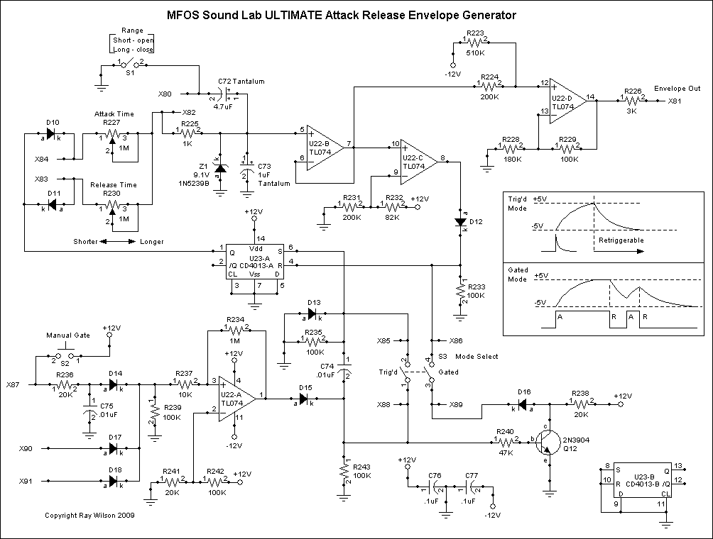
Sound Lab ULTIMATE Attack Release Generator Table Of Contents
Circuit Description
The Sound Lab ULTIMATE AR generator works in two modes: Gated mode or Triggered mode. In gated mode the circuit depends on a gate type signal being fed into the "GATE/TRIG IN" input. That is the gate input should go high (greater than 2.5V) when a key is pressed and low (less than 2V) when it is released. The envelope generator works as an AR (Attack - Release) generator when in gated mode. When the gate is maintained the output rises from -5V to +5V (at a rate set by the ATTACK control) and remains at +5V as long as the gate is maintained. When the gate is released the output falls toward -5V (at a rate set by the RELEASE control). If the gate is applied but released prior to the output reaching +5V the output falls from it's current output voltage back towards -5V (at a rate set by the RELEASE control). Applying the gate again before the output falls completely to -5V causes the output to begin rising back toward +5V from it's current voltage (at a rate set by the ATTACK control).
In triggered mode either a gate or a trigger signal (a trigger signal being a pulse that occurs any time a new key is pressed) can be fed into the "GATE/TRIG IN" input. Only the leading edge of the pulse fed into the "GATE/TRIG IN" input is used in triggered mode. Once the AR is triggered it's output will climb to and attain +5V at which time the release cycle will start. If the trigger is applied again prior to the end of the release cycle (output falling to -5V) the output will climb to and attain +5V and then enter the release cycle again.
The gate/trigger conditioning circuit U22-A and associated components comprise a comparator whose output goes high when the voltage fed to it's non-inverting input (U22-A pin 3) goes above the threshold set by R241 and R242 (about 2V plus some hysteresis due to R234). There are three inputs to the gate/trigger conditioner: X87 is the manual gate input, X90 connects to the front panel banana jack and X91 connects to the 1/4" jack on the auxiliary panel. Each input is fed into the comparator via a diode to isolate the inputs from one another. R36 and C75 act as a low pass filter to clean up the noise of the Manual Gate push button S2 (SPST N.O. push button) The filtering in conjunction with the schmitt trigger action of U22-A (due to hysteresis provided by R234) does a good job of debouncing the manual gate button. Pressing S2 gates the AR generator. When any of the inputs are brought high the output of U22-A goes from -11V to +11V and stays there until all of the inputs are brought low.
Gated mode
The heart of the AR generator is U23-A (one half of a CD4013 CMOS D Flip Flop). Only half of the chip is used U23-B is unused and it's inputs are grounded to keep it quiet. In gated mode when the output of U22-A (pin 1) goes high (-11V to +11V) D15 is forward biased and the above ground excursion of U22-A is fed via D15 to be dropped on R243. This voltage makes it's way through S3 DPST switch (which is closed in gated mode) to the Set (S) input of U23-A. With the gate maintained high transistor Q12 is turned on shunting the current through R238 to ground which effectively keeps U23-A's Reset (R) input at ground. Under these conditions the Q output of U23-A goes high and C73 (in parallel with C72 if the Range switch is set to Long (closed)) begins to charge toward 12V via forward biased D10 and R227 1M log taper Attack Time pot (wired as a variable resistor). The voltage on C73 cannot exceed the level clamped by Z1 (1N5239B 9.1V zener diode). A great characteristic of the 1N5239B zener is that it clamps the voltage accurately regardless of whether the current through it is in the uA range or the mA range. The voltage on C73 is buffered by high impedance non-inverting buffer U22-B (TL074 JFET op amp). U22-B's output is level shifted and increased slightly by U22-D to cause the circuit's envelope output to range from -5V to +5V. Comparator U22-C's output goes high when the voltage on it's non-inverting input goes above the threshold on it's inverting input set by R231 and R232 (about +8.5V). In gated mode the high level held on the Set (S) input of flip flop U23-A keeps the Q output high even if comparator U22-C is applying a high level to the Reset (R) input of flip flop U23-A via D12. When all gate/trig inputs are released (brought low) the output of U22-A goes low which allows the base of Q12 to see a ground through R243 in series with R240. This turns Q12 off so that the current through R238 that was previously shunted to ground now causes about 10 volts to be dropped across R233 which resets the flip flop bringing U23-A's Q output low. When the Q output is low cap C73 discharges to ground at the rate set by Release Time pot R230 (1M log taper).
Triggered mode
In triggered mode S3 is open so that only the leading edge of the buffered gate dropped across R243 is applied to the Set (S) input of U23-A (via C74). If U23-A flip flop was not already set (Q output high) by a previous trigger it becomes set now. In triggered mode this cause C73 to charge toward 12V at the rate set by Attack Time pot R227. When the output of U22-B, which is buffering the voltage on C73, reaches the threshold set by R231 and R232 (about 8.5 volts) U22-C's output goes high, resetting U23-A, via D12, causing C73 to discharge toward ground at the rate set by Release Time pot R230 (1M log taper). In triggered mode the AR generator can be re-triggered any time after the release cycle starts.
S1 (SPST switch) allows C72 to be placed in parallel with C73 to lengthen attack and release times. Times of between 1mS to 10 seconds can be adjusted by means of S1, R227, and R230. The envelope generator's output (X81) is fed to two front panel banana jacks.
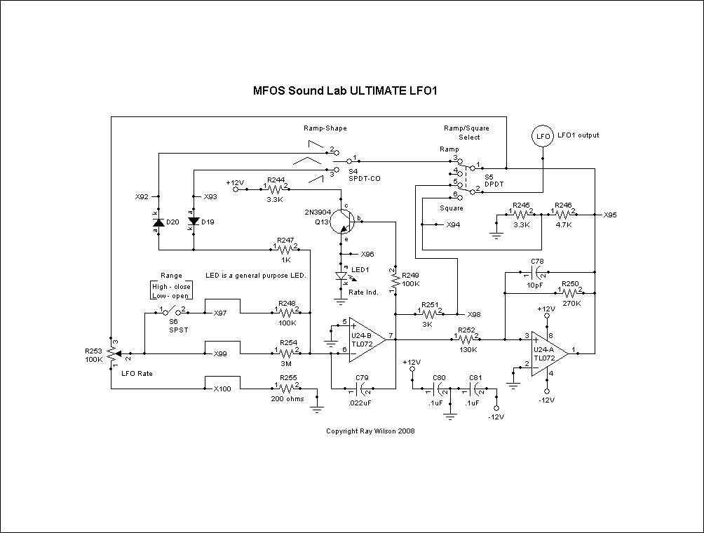
Sound Lab ULTIMATE LFO-1 Table Of Contents
Circuit Description
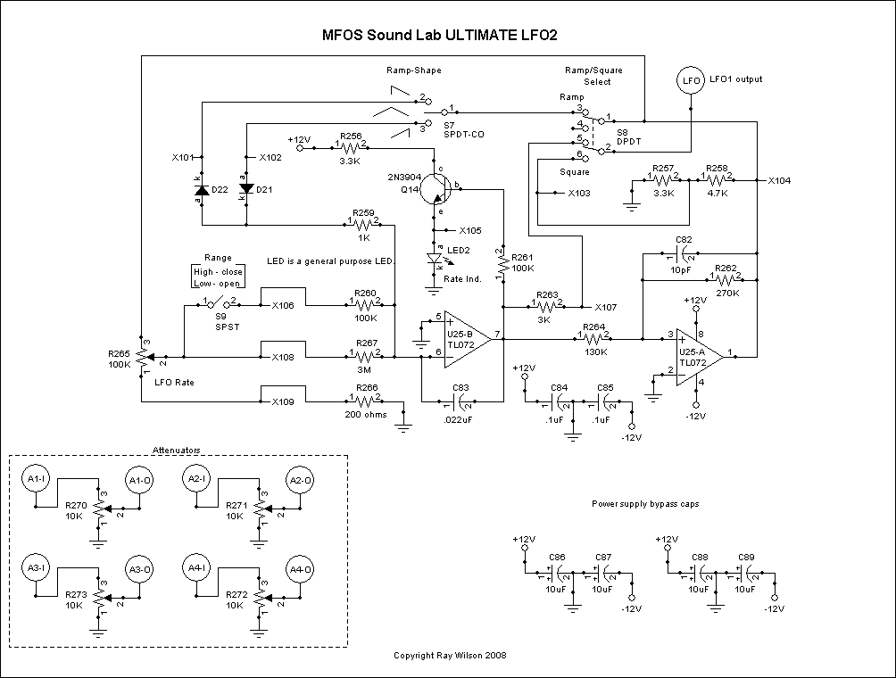
The Sound Lab ULTIMATE contains two identical LFOs. LFO1 and LFO2 differ only in component designators so I will only describe the operation of LFO1.
LFO1 is a simple oscillator built from an integrator and a comparator. U24-B is the integrator. The output of the comparator is fed to the top of R265 (100K linear pot) which is wired as a voltage divider. A portion of the comparator's output voltage is fed to the integrator's input resistors. This pot determines the frequency of the LFO's oscillation.
The current that flows from the wiper of R265 through R254 (3M resistor) determines the rate at which the output of the integrator ramps up or down. Switch S6 SPST allows R248 (100K resistor) to be placed in parallel with R254 when it is closed. This provides a coarse range control function. When S6 is closed (High Range) the LFO goes from a few Hz to about 300 Hz. When S6 is open (Low Range) the LFO goes from a cycle every 10 seconds or so to about 30 Hz. This provides a wide range of modulation options. U24-A is the comparator and when power is applied to the circuit it's output is either high (+11V) or low (-11V) (it does not matter). We will consider the case of when it comes up high.
The output of U24-A is connected to one of the commons of S5 (DPDT switch) and one end of the LFO rate pot R253 (100K linear taper pot). R253 applies a portion of the voltage on the output of U24-A to the integrator via R254 (if S6 is open) or R254 in parallel with R248 (if S6 is closed). The setting of pot R253 determines the current that flows to the integrator (U24-B with C79 in it's negative feedback path) and thus the rate at which the output of U24-B ramps toward -11V. Once the output of U24-B ramps lower than ground plus the ample hysteresis provided by the positive feedback in the comparator (to about -5V) the comparator's output goes low (-11V). Now current is being pulled out of the integrator and U24-B's output ramps high until it reaches the positive threshold of comparator U24-A (about +5V) and the comparator's output goes back high and the cycle repeats resulting in oscillation.
The output of the LFO is controlled by S5. With S5 (DPDT switch) set to Square mode the output of comparator U24-A is routed to the output via R246. R246 and R245 reduce the +/-11 volt output of the comparator to about +/-5V. Triangle wave selector switch S4 (SPDT center off) is taken out of the feedback circuit by the other half of switch S5 DPDT. This is because in Ramp or Sawtooth wave mode the waveform at the output of the comparator is not square but instead is a narrow high going (Ramp mode) or low going (Sawtooth mode) pulse that is not useful for modulation.
With S5 set to Ramp mode the output of the integrator is fed to the output via R251 (3K resistor). The Ramp-Shape selector is placed into the circuit by the other half of S5 and the user can use S4 to select a sawtooth wave (D20 in series with R247 placed in the feedback loop), a triangle wave (neither diode in the feedback loop), or ramp wave (D19 in series with R247 placed in the feedback loop). With a diode in the feedback loop from comparator output to integrator input the integrator is forced to ramp quickly either high or low depending on the setting of S4.
With S4 set to Sawtooth current through D20 in series with 1K resistor R247 when the output of the comparator is low causes the integrator to ramp high in about a millisecond which forces the comparator back high again. When the comparator is high D20 is reverse biased and current to the integrator (and the rate at which it ramps low) depends on the setting of LFO Rate pot R253 and the setting of Range switch S6 SPST.
With S4 set to Ramp current through D19 in series with 1K resistor R247 when the output of the comparator is high causes the integrator to ramp low in about a millisecond which forces the comparator back low again. When the comparator is low D19 is reverse biased and current to the integrator (and the rate at which it ramps high) depends on the setting of LFO Rate pot R253 and the setting of Range switch S6 SPST.
The oscillator's rate increased by a factor of two when either Sawtooth or Ramp are selected when in Ramp mode. This is due to the fact that either the rising or falling half of the triangle wave is eliminated in these modes.
The output of LFO1 is hard wired to the LFO-1 MOD pot of the VCF and brought out to two banana jacks on the panel. LED1 provides a visual indication of the rate of LFO1.
Sound Lab ULTIMATE LFO-2 Table Of Contents
Circuit Description
The description of LFO2 is the same as for LFO1 only the names have been changed to protect the innocent.
The output of LFO2 is hard wired to the LFO-2 MOD pot of the VCA and brought out to two banana jacks on the panel. LED2 provides a visual indication of the rate of LFO2.
The Attenuators (R270, R271, R272, and R273) are simply pots wired as variable voltage dividers that can be used to attenuate anything that you want to use to modulate anything else. Plug from any output to the input of an attenuator and then from the attenuator's output to whatever you want to modulate. The attenuator will provide a level control for the modulation source.
I used two colors of banana jacks on my prototype so that inputs and outputs are readily identifiable. I bought banana plugs from Mouser and made my own cables using the plugs and stranded hookup wire. This was an economical way to get the number of cables I wanted.
Please note that you can order a variety of colors for both the banana jacks and the banana plugs from Mouser. Find the banana plug or jack in the Mouser pre-populated cart and then click on the part number. You will eventually find a link to the catalog page associated with the part where you will see the list of part numbers associated with the various colors.
VCO Scale Calibration
Each of the VCOs needs to be calibrated so that the scale factor is correct (1V/octave). You will need an accurate DVM and a frequency counter. In lieu of a frequency counter your ears or another keyboard can be used to determine when each oscillator is correctly "tuned". You will also need an accurate voltage source. An analog keyboard controller or MIDI to CV module that is in good calibration is the best. You will need to be able to apply at a minimum 0,1,2 and 3 volts with an accuracy of +/-2mV at least.
For example:
- at the 0V setting you will want your DVM to read between -.002V and +.002V,
- at the 1V setting you will want your DVM to read between +0.998V and 1.002V,
- at the 2V setting you will want your DVM to read between +1.998V and +2.002V,
- at the 3V setting you will want your DVM to read between +2.998V and +2.002V.
The closer to the ideal (0.000, 1.000, 2.000 and 3.000) the better.
Each voltage controlled oscillator has both a 100 ohm scale adjust trimmer (VCO-1 -> R11, VCO-2 -> R57, VCO-3 -> R99) and a 100K high frequency compensation trimmer (VCO-1 -> R8, VCO-2 -> R54, VCO-3 -> R96). I will describe the calibration procedure for VCO-1. The same procedure will be used for all VCOs but, of course, using each oscillator's respective trimmers.
You can observe/probe the VCO output at the main output of the unit. That is why all other sound sources and modulation sources need to be OFF. If you prefer you can observe/probe the output of each oscillator separately with you oscilloscope by probing:
- VCO1 - U4-A pin 1
- VCO2 - U8-A pin 1
- VCO3 - U12-A pin 1
Only one LOG-CV input should be applied to each VCO during calibration and all other inputs to the VCO should be disconnected (i.e. remove any connected banana cables from the jacks). At the start of the calibration procedure for each oscillator the high frequency compensation trimmer should be set so that the maximum resistance is between pins 3 and 2. At this setting the pot has the minimum effect on the VCO's V-to-F response.
- Let the synth acclimate to the room's temperature under power for at least half an hour before beginning the procedure.
- Turn all mixer inputs full counter-clockwise (off).
- Turn the VCF initial cut-off frequency and the VCA initial amplitude all the way up and all VCF and VCA modulators down.
- Turn the mixer input for VCO-1 fully clockwise (on).
- Apply 0 volts to one of VCO-1's LOG-CV inputs.
- Use VCO-1's coarse and fine frequency controls to set it's frequency to 100 HZ.
- Increase the voltage being applied to the VCO-1's LOG-CV input to 3 volts.
- The scale adjust trimmer will need to be adjusted to achieve a change of from 100 Hz to 800 Hz when the voltage is increased.
- Tweak the scale adjust trimmer while you alternate the voltage being applied to VCO-1's LOG-CV input between 0V and 3V until the change in frequency is correct.
- Use VCO-1's coarse and fine frequency controls to set it's frequency to 800 HZ.
- Apply 0 volts to one of VCO-1's LOG-CV inputs.
- Increase the voltage being applied to the VCO-1's LOG-CV input to 2 volts.
- The scale adjust trimmer and the high frequency compensation trimmer will need to be adjusted to achieve a change of from 800 Hz to 3200 Hz when the voltage is increased.
- Tweak the scale adjust trimmer and the high frequency compensation trimmer while you alternate the voltage being applied to VCO-1's LOG-CV input between 0V and 2V until the change in frequency is correct.
Repeat the procedure for each of the VCOs adjusting their respective trimmers. Remember to turn the mixer channel for the oscillator you are tuning up and the others down. You will REALLY be mad if you spend 30 minutes adjusting VCO-1 and then when you start calibrating VCO-2 you BY MISTAKE turn VCO-1's trimmers AGAIN!!!. So maybe put a sticky note over them or something to avoid this time consuming disaster (don't ask me how I know this). When all is said and done each VCO should respond so that each change in 1V applied to it's LOG-CV input results in a change in frequency of 1 octave.
This procedure it iterative, the adjustments are sensitive and the trim pots are somewhat interactive. Be prepared to take your time doing this and know that what I have described is the "ideal". You will finally arrive at a tradeoff in which the lower octaves are more in tune than the upper ones but with careful adjustment you will be able to achieve a very in tune musical range 20Hz to 2560Hz for the VCOs. With careful adjustment even higher registers can be scaled properly.
YouTubes about oscillator calibration in general...
VCF Scale Calibration
The ULTIMATE's Low Pass VCF will oscillate when the resonance control is advanced toward maximum. The waveform is a very nice sine wave. You can adjust the VCF's V-to-F response so that the oscillator tracks 1V/oct over a limited range. To do so follow this procedure.
- Let the synth acclimate to the room's temperature under power for at least half an hour before beginning the procedure.
- Turn all mixer inputs fully counter-clockwise (off).
- Turn the AR MOD and LFO-1 MOD for the VCF all the way off (counter clockwise).
- Apply 0 volts to one of VCF's EXT-CV input (disconnect the other EXT-CV input (i.e. remove any connected banana cable from the other jack)).
- Advance the VCF's RESONANCE control until the VCF begins stable oscillation.
- Use the VCF's INITIAL CUTOFF control to set it's frequency to 200 HZ.
- Increase the voltage being applied to the VCF's EXT-CV input to 2 volts.
- The VCF's 100 ohm scale adjust trimmer R280 will need to be adjusted to achieve a change of from 200 Hz to 800 Hz when the voltage is increased.
- Tweak the scale adjust trimmer while you alternate the voltage being applied to VCF's EXT-CV input between 0V and 2V until the change in frequency is as close as possible to this ideal.
VCA CV Null and Output Offset Null Adjustment
The ULTIMATE's VCA has two trimmers R195 (2K CV Null) and R198 (100K Output Offset Null) which should be adjusted for best performance.
R198 (100K Output Offset Null)
- Let the synth acclimate to the room's temperature under power for at least half an hour before beginning the procedure.
- Turn all mixer inputs full counter-clockwise (off).
- Turn the AR MOD and LFO-2 MOD for the VCA all the way off (counter clockwise).
- Disconnect both EXT-CV inputs (i.e. remove any connected banana cables from the jacks).
- Carefully connect a DVM to pin 8 of U18 (LM13700) using a microhook or probe.
- While observing the voltage on pin 8 of U18 (LM13700) adjust R198 until your DVM reads as close to 0V as you can get.
R195 (2K CV Null)
- Let the synth acclimate to the room's temperature under power for at least half an hour before beginning the procedure.
- Turn all mixer inputs full counter-clockwise (off).
- Turn the AR MOD and LFO-2 MOD for the VCA all the way off (counter clockwise).
- Disconnect both EXT-CV inputs (i.e. remove any connected banana cables from the jacks).
- Set LFO-2 to output square wave, RANGE to HIGH and RATE fully clockwise.
- Adjust the VCA's LFO-2 MOD pot to maximum.
- Set your oscilloscope for 10mS per horizontal division and 100mV per vertical division to start (adjust as necessary).
- Carefully connect a scope probe to pin 8 of U18 (LM13700) using a microhook or probe.
- You should observe an artifact of LFO-2 on the output of U18 (LM13700 pin 8).
- While observing the output of U18 (LM13700 pin 8) adjust R195 until the minimum possible amplitude of the artifact is achieved.
Noise Amplitude Adjustment
The ULTIMATE's White Noise Generator has an amplitude trimmer which should be adjusted for proper white noise amplitude. Just a note on noise. I have found that selected 2N5172 transistors produce excellent noise. I bought 1000 of them and have found that about 1 in 5 produce high quality high amplitude noise. While selected 2N3904 transistors will produce good noise if you like you can purchase a pre-selected 2N5172 noise transistor from the "SYNTHFOOL" site SYNTHFOOL selected 2N5172 noise transistor. Just make sure you install it on the board correctly so that the emitter and base pins are oriented properly. The collector can be removed.
- Observing U14 pin 1 (output of the noise generator) with an oscilloscope (10mS per div and 2V per div).
- While observing U14 pin 1 adjust 20K trimmer R144 until the amplitude of the observed noise signal is solidly observed to be about 5 to 6 volts peak to peak with maximum peaks extending to about 10 volts peak to peak.